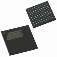
AT89C51SND2C-7FTUL Atmel, AT89C51SND2C-7FTUL Datasheet - Page 7

AT89C51SND2C-7FTUL
Manufacturer Part Number
AT89C51SND2C-7FTUL
Description
IC 8051 MCU FLASH 64K MP3 100BGA
Manufacturer
Atmel
Series
89Cr
Datasheet
1.AT89C51SND2C-7FTUL.pdf
(242 pages)
Specifications of AT89C51SND2C-7FTUL
Core Processor
8051
Core Size
8-Bit
Speed
40MHz
Connectivity
I²C, IDE/ATAPI, MMC, SPI, UART/USART, USB
Peripherals
Audio, I²S, MP3, PCM, POR, WDT
Number Of I /o
32
Program Memory Size
64KB (64K x 8)
Program Memory Type
FLASH
Ram Size
2.25K x 8
Voltage - Supply (vcc/vdd)
2.7 V ~ 3.3 V
Data Converters
A/D 2x10b; D/A 2x20b
Oscillator Type
Internal
Operating Temperature
-40°C ~ 85°C
Package / Case
100-TFBGA
Data Bus Width
8 bit
Data Ram Size
2.25 KB
Interface Type
ATAPI, I2S, IDE, SPI, UART, USB
Maximum Clock Frequency
40 MHz
Number Of Programmable I/os
32
Number Of Timers
2
Maximum Operating Temperature
+ 85 C
Mounting Style
SMD/SMT
Minimum Operating Temperature
- 40 C
Lead Free Status / RoHS Status
Lead free / RoHS Compliant
Eeprom Size
-
Lead Free Status / Rohs Status
Details
Other names
AT89C51SND2C7FTUL
Available stocks
Company
Part Number
Manufacturer
Quantity
Price
Company:
Part Number:
AT89C51SND2C-7FTUL
Manufacturer:
ATMEL
Quantity:
4 371
- Current page: 7 of 242
- Download datasheet (3Mb)
4341H–MP3–10/07
Table 4-4.
Table 4-5.
Table 4-6.
Signal
Signal
Signal
Signal
MCMD
DOUT
Name
Name
DCLK
Name
Name
MCLK
MDAT
DSEL
SCLK
INT1
D+
T0
T1
D-
Type
Type
Type
Type
I/O
I/O
I/O
I/O
O
O
O
O
O
I
I
I
Audio Interface Signal Description
USB Controller Signal Description
MutiMediaCard Interface Signal Description
Description
Timer 1 Gate Input
INT1 serves as external run control for timer 1, when selected by GATE1 bit in
TCON register.
External Interrupt 1
INT1 input sets IE1 in the TCON register. If bit IT1 in this register is set, bit IE1
is set by a falling edge on INT1#. If bit IT1 is cleared, bit IE1 is set by a low
level on INT1#.
Timer 0 External Clock Input
When timer 0 operates as a counter, a falling edge on the T0 pin increments
the count.
Timer 1 External Clock Input
When timer 1 operates as a counter, a falling edge on the T1 pin increments
the count.
Description
DAC Data Bit Clock
DAC Audio Data Output
DAC Channel Select Signal
DSEL is the sample rate clock output.
DAC System Clock
SCLK is the oversampling clock synchronized to the digital audio data (DOUT)
and the channel selection signal (DSEL).
Description
USB Positive Data Upstream Port
This pin requires an external 1.5 KΩ pull-up to V
USB Negative Data Upstream Port
Description
MMC Clock output
Data or command clock transfer.
MMC Command line
Bidirectional command channel used for card initialization and data transfer
commands. To avoid any parasitic current consumption, unused MCMD input
must be polarized to V
MMC Data line
Bidirectional data channel. To avoid any parasitic current consumption, unused
MDAT input must be polarized to V
DD
or V
SS
.
DD
or V
AT8xC51SND2C/MP3B
SS
.
DD
for full speed operation.
Alternate
Alternate
Alternate
Alternate
Function
Function
Function
Function
P3.3
P3.4
P3.5
-
-
-
-
-
-
-
-
-
7
Related parts for AT89C51SND2C-7FTUL
Image
Part Number
Description
Manufacturer
Datasheet
Request
R

Part Number:
Description:
DEV KIT FOR AVR/AVR32
Manufacturer:
Atmel
Datasheet:

Part Number:
Description:
INTERVAL AND WIPE/WASH WIPER CONTROL IC WITH DELAY
Manufacturer:
ATMEL Corporation
Datasheet:

Part Number:
Description:
Low-Voltage Voice-Switched IC for Hands-Free Operation
Manufacturer:
ATMEL Corporation
Datasheet:

Part Number:
Description:
MONOLITHIC INTEGRATED FEATUREPHONE CIRCUIT
Manufacturer:
ATMEL Corporation
Datasheet:

Part Number:
Description:
AM-FM Receiver IC U4255BM-M
Manufacturer:
ATMEL Corporation
Datasheet:

Part Number:
Description:
Monolithic Integrated Feature Phone Circuit
Manufacturer:
ATMEL Corporation
Datasheet:

Part Number:
Description:
Multistandard Video-IF and Quasi Parallel Sound Processing
Manufacturer:
ATMEL Corporation
Datasheet:

Part Number:
Description:
High-performance EE PLD
Manufacturer:
ATMEL Corporation
Datasheet:

Part Number:
Description:
8-bit Flash Microcontroller
Manufacturer:
ATMEL Corporation
Datasheet:

Part Number:
Description:
2-Wire Serial EEPROM
Manufacturer:
ATMEL Corporation
Datasheet:


