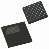
AT89C51SND2C-7FTUL Atmel, AT89C51SND2C-7FTUL Datasheet - Page 132

AT89C51SND2C-7FTUL
Manufacturer Part Number
AT89C51SND2C-7FTUL
Description
IC 8051 MCU FLASH 64K MP3 100BGA
Manufacturer
Atmel
Series
89Cr
Datasheet
1.AT89C51SND2C-7FTUL.pdf
(242 pages)
Specifications of AT89C51SND2C-7FTUL
Core Processor
8051
Core Size
8-Bit
Speed
40MHz
Connectivity
I²C, IDE/ATAPI, MMC, SPI, UART/USART, USB
Peripherals
Audio, I²S, MP3, PCM, POR, WDT
Number Of I /o
32
Program Memory Size
64KB (64K x 8)
Program Memory Type
FLASH
Ram Size
2.25K x 8
Voltage - Supply (vcc/vdd)
2.7 V ~ 3.3 V
Data Converters
A/D 2x10b; D/A 2x20b
Oscillator Type
Internal
Operating Temperature
-40°C ~ 85°C
Package / Case
100-TFBGA
Data Bus Width
8 bit
Data Ram Size
2.25 KB
Interface Type
ATAPI, I2S, IDE, SPI, UART, USB
Maximum Clock Frequency
40 MHz
Number Of Programmable I/os
32
Number Of Timers
2
Maximum Operating Temperature
+ 85 C
Mounting Style
SMD/SMT
Minimum Operating Temperature
- 40 C
Lead Free Status / RoHS Status
Lead free / RoHS Compliant
Eeprom Size
-
Lead Free Status / Rohs Status
Details
Other names
AT89C51SND2C7FTUL
Available stocks
Company
Part Number
Manufacturer
Quantity
Price
Company:
Part Number:
AT89C51SND2C-7FTUL
Manufacturer:
ATMEL
Quantity:
4 371
- Current page: 132 of 242
- Download datasheet (3Mb)
17.1.1
132
AT8xC51SND2C/MP3B
IDE Device Connection
Figure 17-2. IDE Write Waveforms
Notes:
Figure 17-3 and Figure 17-4 show 2 examples on how to interface up to 2 IDE devices to the
AT8xC51SND2C. In both examples P0 carries IDE low order data bits D7:0, P2 carries IDE high
order data bits D15:8, while RD and WR signals are respectively connected to the IDE nIOR and
nIOW signals. Other IDE control signals are generated by the external address latch outputs in
the first example while they are generated by some port I/Os in the second one. Using an exter-
nal latch will achieve higher transfer rate.
Figure 17-3. IDE Device Connection Example 1
Figure 17-4. IDE Device Connection Example 2
1.
2. When executing MOVX @Ri instruction, P2 outputs SFR content.
3. When executing MOVX @DPTR instruction, if DPHDIS is set (Page Access Mode), P2 out-
CPU Clock
WR
puts SFR content instead of DPH.
AT8xC51SND2C
AT8xC51SND2C
WR
ALE
signal may be stretched using M0 bit in AUXR register.
P0
P2
(1)
P0/AD7:0
P2/A15:8
P4.2:0
P4.4:3
P4.5
Px.y
ALE
WR
WR
RD
RD
P2
P0
P2
DPH or P2
DPL or Ri
Latch
(2),(3)
D15-8
D7:0
A2:0
nCS1:0
nRESET
nIOR
nIOW
D15-8
D7:0
A2:0
nCS1:0
nRESET
nIOR
nIOW
IDE Device 0
IDE Device 0
D15:8
D7:0
D15-8
D7:0
A2:0
nCS1:0
nRESET
nIOR
nIOW
D15-8
D7:0
A2:0
nCS1:0
nRESET
nIOR
nIOW
IDE Device 1
IDE Device 1
4341H–MP3–10/07
P2
Related parts for AT89C51SND2C-7FTUL
Image
Part Number
Description
Manufacturer
Datasheet
Request
R

Part Number:
Description:
DEV KIT FOR AVR/AVR32
Manufacturer:
Atmel
Datasheet:

Part Number:
Description:
INTERVAL AND WIPE/WASH WIPER CONTROL IC WITH DELAY
Manufacturer:
ATMEL Corporation
Datasheet:

Part Number:
Description:
Low-Voltage Voice-Switched IC for Hands-Free Operation
Manufacturer:
ATMEL Corporation
Datasheet:

Part Number:
Description:
MONOLITHIC INTEGRATED FEATUREPHONE CIRCUIT
Manufacturer:
ATMEL Corporation
Datasheet:

Part Number:
Description:
AM-FM Receiver IC U4255BM-M
Manufacturer:
ATMEL Corporation
Datasheet:

Part Number:
Description:
Monolithic Integrated Feature Phone Circuit
Manufacturer:
ATMEL Corporation
Datasheet:

Part Number:
Description:
Multistandard Video-IF and Quasi Parallel Sound Processing
Manufacturer:
ATMEL Corporation
Datasheet:

Part Number:
Description:
High-performance EE PLD
Manufacturer:
ATMEL Corporation
Datasheet:

Part Number:
Description:
8-bit Flash Microcontroller
Manufacturer:
ATMEL Corporation
Datasheet:

Part Number:
Description:
2-Wire Serial EEPROM
Manufacturer:
ATMEL Corporation
Datasheet:


