IP-PCIE/1 Altera, IP-PCIE/1 Datasheet - Page 341
IP-PCIE/1
Manufacturer Part Number
IP-PCIE/1
Description
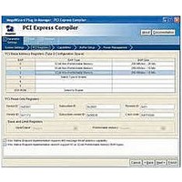
IP CORE - PCI Express X1 Lane
Manufacturer
Altera
Type
MegaCorer
Specifications of IP-PCIE/1
Software Application
IP CORE, Interface And Protocols, PCI
Supported Families
Arria GX, Cyclone II, HardCopy II, Stratix II
Core Architecture
FPGA
Core Sub-architecture
Arria, Cyclone, Stratix
Rohs Compliant
NA
Function
PCI Express Compiler, x1 Link Width
License
Initial License
Lead Free Status / RoHS Status
na
Lead Free Status / RoHS Status
na


Chapter :
Recommended Incremental Compilation Flow
Figure B–26. TX Interface Timing Diagram
Table B–16. MSI TX Signals
Figure B–27. MSI Interface Timing Diagram
December 2010 Altera Corporation
msi_stream_valid0
msi_stream_data0
msi_stream_ready0
tx_stream_ready0
tx_stream_valid0
msi_stream_ready0
Signal
msi_stream_valid0
msi_stream_data0
tx_sop_flag
tx_eop_flag
tx_desc0
tx_data0
clk
clk
Figure B–26
Table B–16
Figure B–27
1
1
63:8
7:5
4:0
Bit
2
2
describes the MSI TX signals.
Subsignals
shows the application-side TX interface timing diagram.
shows the application-side MSI interface timing diagram.
3
3
4
4
Clocks msi_st_data into the ICM.
msi data.
Corresponds to the app_msi_tc signal on the IP core. Refer to
on page 5–29
Corresponds to the app_msi_num signal on the IP core. Refer to
Table 5–9 on page 5–29
The ICM asserts this signal when it can accept more MSI requests. When
deasserted, the application must deassert msi_st_valid within 3 CLK
cycles.
5
5
6
6
desc_hi desc_lo data0
for more information.
7
7
response time
0 - 3 clocks
allowed
for more information.
8
8
msi1
response time
Description
0 - 3 clocks
allowed
9
9
data1
10
10
11
PCI Express Compiler User Guide
11
throttles
source
data
msi2
12
12
last data
13
13
Table 5–9
14
B–35
Related parts for IP-PCIE/1
Image
Part Number
Description
Manufacturer
Datasheet
Request
R

Part Number:
Description:
IP CORE - 32-bit 66MHz PCI Master/Target
Manufacturer:
Altera
Datasheet:
Part Number:
Description:
IP CORE - 64-bit 66MHz PCI Master/Target
Manufacturer:
Altera
Datasheet:
Part Number:
Description:
IP CORE - 32-bit 66MHz PCI Target
Manufacturer:
Altera
Datasheet:
Part Number:
Description:
IP CORE - 64-bit 66MHz PCI Target
Manufacturer:
Altera
Datasheet:
Part Number:
Description:
IP CORE Renewal Of IP-PCI/MT32
Manufacturer:
Altera
Datasheet:
Part Number:
Description:
IP CORE Renewal Of IP-PCI/MT64
Manufacturer:
Altera
Datasheet:
Part Number:
Description:
IP CORE Renewal Of IP-PCI/T32
Manufacturer:
Altera
Datasheet:
Part Number:
Description:
IP CORE Renewal Of IP-PCI/T64
Manufacturer:
Altera
Datasheet:

Part Number:
Description:
IP CORE - PCI Express X1 And X4 Lanes
Manufacturer:
Altera
Datasheet:
Part Number:
Description:
IP CORE - PCI Express X1 X4 And X8 Lanes
Manufacturer:
Altera
Datasheet:
Part Number:
Description:
IP NIOS II MEGACORE
Manufacturer:
Altera
Datasheet:
