IP-PCIE/1 Altera, IP-PCIE/1 Datasheet - Page 48
IP-PCIE/1
Manufacturer Part Number
IP-PCIE/1
Description
IP CORE - PCI Express X1 Lane
Manufacturer
Altera
Type
MegaCorer
Specifications of IP-PCIE/1
Software Application
IP CORE, Interface And Protocols, PCI
Supported Families
Arria GX, Cyclone II, HardCopy II, Stratix II
Core Architecture
FPGA
Core Sub-architecture
Arria, Cyclone, Stratix
Rohs Compliant
NA
Function
PCI Express Compiler, x1 Link Width
License
Initial License
Lead Free Status / RoHS Status
na
Lead Free Status / RoHS Status
na


3–6
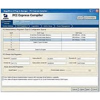
Table 3–2. PCI Registers (Part 2 of 2)
Capabilities Parameters
PCI Express Compiler User Guide
Subsystem vendor ID
0x02C (3)
Class code
0x008
Input/Output
Prefetchable memory
Notes to
(1) A prefetchable 64-bit BAR is supported. A non-prefetchable 64-bit BAR is not supported because in a typical system, the root port configuration
(2) The SOPC Builder flow does not support I/O space for BAR type mapping. I/O space is only supported for legacy endpoint port types.
(3) Only available for EP designs which require the use of the Header type 0 PCI configuration register.
(4) The SOPC Builder flow does not support the expansion ROM.
(5) Only available for RP designs which require the use of the Header type 1 PCI configuration register.
(5)
register of type 1 sets the maximum non-prefetchable memory window to 32-bits.
Table
3–2:
(5)
The Capabilities page contains the parameters setting various capability properties of
the IP core. These parameters are described in
stored in the
Common Configuration Space Header
0x1172
0xFF0000
Disable
16-bit I/O addressing
32-bit I/O addressing
Disable
32-bit I/O addressing
64-bit I/O addressing
Common Configuration Space
Base and Limit Registers
Sets the read-only value of the subsystem vendor ID register. This
parameter can not be set to 0xFFFF per the
Specification 1.1 or
Sets the read-only value of the class code register.
IO limit registers.
Specifies what address widths are supported for the prefetchable
memory base register and prefetchable memory limit register.
Specifies what address widths are supported for the IO base and
indicates the parameter address.
2.0.
Header. The byte offset within the
Table
3–3. Some of these parameters are
December 2010 Altera Corporation
Chapter 3: Parameter Settings
PCI Express Base
Capabilities Parameters
Related parts for IP-PCIE/1
Image
Part Number
Description
Manufacturer
Datasheet
Request
R

Part Number:
Description:
IP CORE - 32-bit 66MHz PCI Master/Target
Manufacturer:
Altera
Datasheet:
Part Number:
Description:
IP CORE - 64-bit 66MHz PCI Master/Target
Manufacturer:
Altera
Datasheet:
Part Number:
Description:
IP CORE - 32-bit 66MHz PCI Target
Manufacturer:
Altera
Datasheet:
Part Number:
Description:
IP CORE - 64-bit 66MHz PCI Target
Manufacturer:
Altera
Datasheet:
Part Number:
Description:
IP CORE Renewal Of IP-PCI/MT32
Manufacturer:
Altera
Datasheet:
Part Number:
Description:
IP CORE Renewal Of IP-PCI/MT64
Manufacturer:
Altera
Datasheet:
Part Number:
Description:
IP CORE Renewal Of IP-PCI/T32
Manufacturer:
Altera
Datasheet:
Part Number:
Description:
IP CORE Renewal Of IP-PCI/T64
Manufacturer:
Altera
Datasheet:

Part Number:
Description:
IP CORE - PCI Express X1 And X4 Lanes
Manufacturer:
Altera
Datasheet:
Part Number:
Description:
IP CORE - PCI Express X1 X4 And X8 Lanes
Manufacturer:
Altera
Datasheet:
Part Number:
Description:
IP NIOS II MEGACORE
Manufacturer:
Altera
Datasheet:
