IP-PCIE/1 Altera, IP-PCIE/1 Datasheet - Page 73
IP-PCIE/1
Manufacturer Part Number
IP-PCIE/1
Description
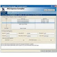
IP CORE - PCI Express X1 Lane
Manufacturer
Altera
Type
MegaCorer
Specifications of IP-PCIE/1
Software Application
IP CORE, Interface And Protocols, PCI
Supported Families
Arria GX, Cyclone II, HardCopy II, Stratix II
Core Architecture
FPGA
Core Sub-architecture
Arria, Cyclone, Stratix
Rohs Compliant
NA
Function
PCI Express Compiler, x1 Link Width
License
Initial License
Lead Free Status / RoHS Status
na
Lead Free Status / RoHS Status
na


Chapter 4: IP Core Architecture
Physical Layer
December 2010 Altera Corporation
The physical layer integrates both digital and analog elements. Intel designed the
PIPE interface to separate the MAC from the PHY. The IP core is compliant with the
PIPE interface, allowing integration with other PIPE-compliant external PHY devices.
Depending on the parameters you set in the parameter editor, the IP core can
automatically instantiate a complete PHY layer when targeting the Arria II GX,
Cyclone IV GX, HardCopy IV GX, Stratix II GX, Stratix IV GX or Stratix V GX devices.
The PHYMAC block is divided in four main sub-blocks:
■
■
■
■
MAC Lane—Both the receive and the transmit path use this block.
■
■
LTSSM—This block implements the LTSSM and logic that tracks what is received
and transmitted on each lane.
■
■
LTSTX (Ordered Set and SKP Generation)—This sub-block generates the physical
layer packet (PLP). It receives control signals from the LTSSM block and generates
PLP for each lane of the core. It generates the same PLP for all lanes and PAD
symbols for the link or lane number in the corresponding TS1/TS2 fields.
Deskew—This sub-block performs the multilane deskew function and the RX
alignment between the number of initialized lanes and the 64-bit data path.
The block also handles the receiver detection operation to the PCS sub-layer by
asserting predefined PIPE signals and waiting for the result. It also generates a
SKIP ordered set at every predefined timeslot and interacts with the TX alignment
block to prevent the insertion of a SKIP ordered set in the middle of packet.
The multilane deskew implements an eight-word FIFO for each lane to store
symbols. Each symbol includes eight data bits and one control bit. The FTS, COM,
and SKP symbols are discarded by the FIFO; the PAD and IDL are replaced by
D0.0 data. When all eight FIFOs contain data, a read can occur.
On the receive side, the block decodes the physical layer packet (PLP) and
reports to the LTSSM the type of TS1/TS2 received and the number of TS1s
received since the LTSSM entered the current state. The LTSSM also reports the
reception of FTS, SKIP and IDL ordered sets and the reception of eight
consecutive D0.0 symbols.
On the transmit side, the block multiplexes data from the data link layer and
the LTSTX sub-block. It also adds lane specific information, including the lane
number and the force PAD value when the LTSSM disables the lane during
initialization.
For transmission, it interacts with each MAC lane sub-block and with the
LTSTX sub-block by asserting both global and per-lane control bits to generate
specific physical layer packets.
On the receive path, it receives the PLPs reported by each MAC lane sub-block.
It also enables the multilane deskew block and the delay required before the TX
alignment sub-block can move to the recovery or low power state. A higher
layer can direct this block to move to the recovery, disable, hot reset or low
power states through a simple request/acknowledge protocol. This block
reports the physical layer status to higher layers.
PCI Express Compiler User Guide
4–15
Related parts for IP-PCIE/1
Image
Part Number
Description
Manufacturer
Datasheet
Request
R

Part Number:
Description:
IP CORE - 32-bit 66MHz PCI Master/Target
Manufacturer:
Altera
Datasheet:
Part Number:
Description:
IP CORE - 64-bit 66MHz PCI Master/Target
Manufacturer:
Altera
Datasheet:
Part Number:
Description:
IP CORE - 32-bit 66MHz PCI Target
Manufacturer:
Altera
Datasheet:
Part Number:
Description:
IP CORE - 64-bit 66MHz PCI Target
Manufacturer:
Altera
Datasheet:
Part Number:
Description:
IP CORE Renewal Of IP-PCI/MT32
Manufacturer:
Altera
Datasheet:
Part Number:
Description:
IP CORE Renewal Of IP-PCI/MT64
Manufacturer:
Altera
Datasheet:
Part Number:
Description:
IP CORE Renewal Of IP-PCI/T32
Manufacturer:
Altera
Datasheet:
Part Number:
Description:
IP CORE Renewal Of IP-PCI/T64
Manufacturer:
Altera
Datasheet:

Part Number:
Description:
IP CORE - PCI Express X1 And X4 Lanes
Manufacturer:
Altera
Datasheet:
Part Number:
Description:
IP CORE - PCI Express X1 X4 And X8 Lanes
Manufacturer:
Altera
Datasheet:
Part Number:
Description:
IP NIOS II MEGACORE
Manufacturer:
Altera
Datasheet:
