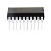
MC68HC908JK8CP Freescale Semiconductor, MC68HC908JK8CP Datasheet - Page 109

MC68HC908JK8CP
Manufacturer Part Number
MC68HC908JK8CP
Description
Manufacturer
Freescale Semiconductor
Datasheet
1.MC68HC908JK8CP.pdf
(212 pages)
Specifications of MC68HC908JK8CP
Cpu Family
HC08
Device Core Size
8b
Frequency (max)
8MHz
Interface Type
SCI
Program Memory Type
Flash
Program Memory Size
8KB
Total Internal Ram Size
256Byte
# I/os (max)
15
Number Of Timers - General Purpose
4
Operating Supply Voltage (typ)
3.3/5V
Operating Supply Voltage (max)
5.5V
Operating Supply Voltage (min)
2.7V
On-chip Adc
13-chx8-bit
Instruction Set Architecture
CISC
Operating Temp Range
-40C to 85C
Operating Temperature Classification
Industrial
Mounting
Through Hole
Pin Count
20
Package Type
PDIP
Lead Free Status / Rohs Status
Not Compliant
Available stocks
Company
Part Number
Manufacturer
Quantity
Price
Company:
Part Number:
MC68HC908JK8CP
Manufacturer:
ALTERA
Quantity:
13
Company:
Part Number:
MC68HC908JK8CPE
Manufacturer:
FREESCALE
Quantity:
928
Part Number:
MC68HC908JK8CPE
Manufacturer:
FREESCALE
Quantity:
20 000
8.4.3.1 Unbuffered Output Compare
Any output compare channel can generate unbuffered output compare pulses as described in
Output
the new value over the old value currently in the TIM channel registers.
An unsynchronized write to the TIM channel registers to change an output compare value could cause
incorrect operation for up to two counter overflow periods. For example, writing a new value before the
counter reaches the old value but after the counter reaches the new value prevents any compare during
that counter overflow period. Also, using a TIM overflow interrupt routine to write a new, smaller output
compare value may cause the compare to be missed. The TIM may pass the new value before it is written.
Use the following methods to synchronize unbuffered changes in the output compare value on channel x:
8.4.3.2 Buffered Output Compare
Channels 0 and 1 can be linked to form a buffered output compare channel whose output appears on the
TCH0 pin. The TIM channel registers of the linked pair alternately control the output.
Setting the MS0B bit in TIM channel 0 status and control register (TSC0) links channel 0 and channel 1.
The output compare value in the TIM channel 0 registers initially controls the output on the TCH0 pin.
Writing to the TIM channel 1 registers enables the TIM channel 1 registers to synchronously control the
output after the TIM overflows. At each subsequent overflow, the TIM channel registers (0 or 1) that
control the output are the ones written to last. TSC0 controls and monitors the buffered output compare
function, and TIM channel 1 status and control register (TSC1) is unused. While the MS0B bit is set, the
channel 1 pin, TCH1, is available as a general-purpose I/O pin.
8.4.4 Pulse Width Modulation (PWM)
By using the toggle-on-overflow feature with an output compare channel, the TIM can generate a PWM
signal. The value in the TIM counter modulo registers determines the period of the PWM signal. The
channel pin toggles when the counter reaches the value in the TIM counter modulo registers. The time
between overflows is the period of the PWM signal.
As
of the PWM signal. The time between overflow and output compare is the pulse width. Program the TIM
Freescale Semiconductor
•
•
Figure 8-3
When changing to a smaller value, enable channel x output compare interrupts and write the new
value in the output compare interrupt routine. The output compare interrupt occurs at the end of
the current output compare pulse. The interrupt routine has until the end of the counter overflow
period to write the new value.
When changing to a larger output compare value, enable TIM overflow interrupts and write the new
value in the TIM overflow interrupt routine. The TIM overflow interrupt occurs at the end of the
current counter overflow period. Writing a larger value in an output compare interrupt routine (at
the end of the current pulse) could cause two output compares to occur in the same counter
overflow period.
Compare. The pulses are unbuffered because changing the output compare value requires writing
shows, the output compare value in the TIM channel registers determines the pulse width
In buffered output compare operation, do not write new output compare
values to the currently active channel registers. User software should track
the currently active channel to prevent writing a new value to the active
channel. Writing to the active channel registers is the same as generating
unbuffered output compares.
MC68HC908JL8/JK8 • MC68HC08JL8/JK8 • MC68HC908KL8 Data Sheet, Rev. 3.1
NOTE
Functional Description
8.4.3
109


