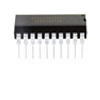
MC68HC908JK8CP Freescale Semiconductor, MC68HC908JK8CP Datasheet - Page 149

MC68HC908JK8CP
Manufacturer Part Number
MC68HC908JK8CP
Description
Manufacturer
Freescale Semiconductor
Datasheet
1.MC68HC908JK8CP.pdf
(212 pages)
Specifications of MC68HC908JK8CP
Cpu Family
HC08
Device Core Size
8b
Frequency (max)
8MHz
Interface Type
SCI
Program Memory Type
Flash
Program Memory Size
8KB
Total Internal Ram Size
256Byte
# I/os (max)
15
Number Of Timers - General Purpose
4
Operating Supply Voltage (typ)
3.3/5V
Operating Supply Voltage (max)
5.5V
Operating Supply Voltage (min)
2.7V
On-chip Adc
13-chx8-bit
Instruction Set Architecture
CISC
Operating Temp Range
-40C to 85C
Operating Temperature Classification
Industrial
Mounting
Through Hole
Pin Count
20
Package Type
PDIP
Lead Free Status / Rohs Status
Not Compliant
Available stocks
Company
Part Number
Manufacturer
Quantity
Price
Company:
Part Number:
MC68HC908JK8CP
Manufacturer:
ALTERA
Quantity:
13
Company:
Part Number:
MC68HC908JK8CPE
Manufacturer:
FREESCALE
Quantity:
928
Part Number:
MC68HC908JK8CPE
Manufacturer:
FREESCALE
Quantity:
20 000
- Current page: 149 of 212
- Download datasheet (2Mb)
ADCO — ADC Continuous Conversion Bit
ADCH[4:0] — ADC Channel Select Bits
Freescale Semiconductor
When set, the ADC will convert samples continuously and update the ADR register at the end of each
conversion. Only one conversion is allowed when this bit is cleared. Reset clears the ADCO bit.
ADCH[4:0] form a 5-bit field which is used to select one of the ADC channels. The five channel select
bits are detailed in the following table. Care should be taken when using a port pin as both an analog
and a digital input simultaneously to prevent switching noise from corrupting the analog signal. (See
Table
The ADC subsystem is turned off when the channel select bits are all set to one. This feature allows
for reduced power consumption for the MCU when the ADC is not used. Reset sets all of these bits to
a logic 1.
1 = Continuous ADC conversion
0 = One ADC conversion
1. If any unused channels are selected, the resulting ADC conversion will be unknown.
2. The voltage levels supplied from internal reference nodes as specified in the table are used to verify the
ADCH4
operation of the ADC converter both in production test and for user applications.
10-1.)
0
0
0
0
0
0
0
0
0
0
0
0
0
0
1
1
1
1
1
1
:
Recovery from the disabled state requires one conversion cycle to stabilize.
MC68HC908JL8/JK8 • MC68HC08JL8/JK8 • MC68HC908KL8 Data Sheet, Rev. 3.1
ADCH3
0
0
0
0
0
0
0
0
1
1
1
1
1
1
1
1
1
1
1
1
:
ADCH2
0
0
0
0
1
1
1
1
0
0
0
0
1
1
0
0
1
1
1
1
:
Table 10-1. MUX Channel Select
ADCH1
0
0
1
1
0
0
1
1
0
0
1
1
0
0
1
1
0
0
1
1
:
NOTE
ADCH0
0
1
0
1
0
1
0
1
0
1
0
1
0
1
0
1
0
1
0
1
:
ADC Channel
ADC10
ADC11
ADC12
ADC0
ADC1
ADC2
ADC3
ADC4
ADC5
ADC6
ADC7
ADC8
ADC9
—
—
—
ADC power off
ADC12/T2CLK
Input Select
Unused
Reserved
Reserved
V
V
PTB0
PTB1
PTB2
PTB3
PTB4
PTB5
PTB6
PTB7
PTD3
PTD2
PTD1
PTD0
DD
SS
(2)
(2)
(1)
I/O Registers
149
Related parts for MC68HC908JK8CP
Image
Part Number
Description
Manufacturer
Datasheet
Request
R
Part Number:
Description:
Manufacturer:
Freescale Semiconductor, Inc
Datasheet:
Part Number:
Description:
Manufacturer:
Freescale Semiconductor, Inc
Datasheet:
Part Number:
Description:
Manufacturer:
Freescale Semiconductor, Inc
Datasheet:
Part Number:
Description:
Manufacturer:
Freescale Semiconductor, Inc
Datasheet:
Part Number:
Description:
Manufacturer:
Freescale Semiconductor, Inc
Datasheet:
Part Number:
Description:
Manufacturer:
Freescale Semiconductor, Inc
Datasheet:
Part Number:
Description:
Manufacturer:
Freescale Semiconductor, Inc
Datasheet:
Part Number:
Description:
Manufacturer:
Freescale Semiconductor, Inc
Datasheet:
Part Number:
Description:
Manufacturer:
Freescale Semiconductor, Inc
Datasheet:
Part Number:
Description:
Manufacturer:
Freescale Semiconductor, Inc
Datasheet:
Part Number:
Description:
Manufacturer:
Freescale Semiconductor, Inc
Datasheet:
Part Number:
Description:
Manufacturer:
Freescale Semiconductor, Inc
Datasheet:
Part Number:
Description:
Manufacturer:
Freescale Semiconductor, Inc
Datasheet:
Part Number:
Description:
Manufacturer:
Freescale Semiconductor, Inc
Datasheet:
Part Number:
Description:
Manufacturer:
Freescale Semiconductor, Inc
Datasheet:


