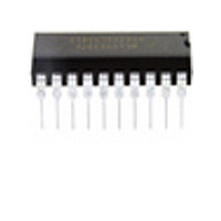
MC68HC908JK8CP Freescale Semiconductor, MC68HC908JK8CP Datasheet - Page 177

MC68HC908JK8CP
Manufacturer Part Number
MC68HC908JK8CP
Description
Manufacturer
Freescale Semiconductor
Datasheet
1.MC68HC908JK8CP.pdf
(212 pages)
Specifications of MC68HC908JK8CP
Cpu Family
HC08
Device Core Size
8b
Frequency (max)
8MHz
Interface Type
SCI
Program Memory Type
Flash
Program Memory Size
8KB
Total Internal Ram Size
256Byte
# I/os (max)
15
Number Of Timers - General Purpose
4
Operating Supply Voltage (typ)
3.3/5V
Operating Supply Voltage (max)
5.5V
Operating Supply Voltage (min)
2.7V
On-chip Adc
13-chx8-bit
Instruction Set Architecture
CISC
Operating Temp Range
-40C to 85C
Operating Temperature Classification
Industrial
Mounting
Through Hole
Pin Count
20
Package Type
PDIP
Lead Free Status / Rohs Status
Not Compliant
Available stocks
Company
Part Number
Manufacturer
Quantity
Price
Company:
Part Number:
MC68HC908JK8CP
Manufacturer:
ALTERA
Quantity:
13
Company:
Part Number:
MC68HC908JK8CPE
Manufacturer:
FREESCALE
Quantity:
928
Part Number:
MC68HC908JK8CPE
Manufacturer:
FREESCALE
Quantity:
20 000
- Current page: 177 of 212
- Download datasheet (2Mb)
Chapter 15
Low Voltage Inhibit (LVI)
15.1 Introduction
This section describes the low-voltage inhibit module (LVI), which monitors the voltage on the V
and generates a reset when the V
15.2 Features
Features of the LVI module include the following:
15.3 Functional Description
Figure 15-1
contains a bandgap reference circuit and comparator. Setting LVI disable bit (LVID) disables the LVI to
monitor V
LVI module should take actions.
The LVI module generates one output signal:
LVI Reset — an reset signal will be generated to reset the CPU when V
point.
Freescale Semiconductor
•
•
Selectable LVI trip voltage
Selectable LVI circuit disable
DD
shows the structure of the LVI module. The LVI is enabled after a reset. The LVI module
voltage. The LVI trip voltage selection bits (LVIT1, LVIT0) determine at which V
LVIT1
MC68HC908JL8/JK8 • MC68HC08JL8/JK8 • MC68HC908KL8 Data Sheet, Rev. 3.1
DETECTOR
LOW V
V
DD
DD
LVIT0
V
V
DD
DD
Figure 15-1. LVI Module Block Diagram
> LVI
< LVI
DD
TRIP
TRIP
voltage falls to the LVI trip (LVI
= 0
= 1
LVID
TRIP
DD
) voltage.
drops to below the set trip
LVI RESET
DD
level the
DD
pin
177
Related parts for MC68HC908JK8CP
Image
Part Number
Description
Manufacturer
Datasheet
Request
R
Part Number:
Description:
Manufacturer:
Freescale Semiconductor, Inc
Datasheet:
Part Number:
Description:
Manufacturer:
Freescale Semiconductor, Inc
Datasheet:
Part Number:
Description:
Manufacturer:
Freescale Semiconductor, Inc
Datasheet:
Part Number:
Description:
Manufacturer:
Freescale Semiconductor, Inc
Datasheet:
Part Number:
Description:
Manufacturer:
Freescale Semiconductor, Inc
Datasheet:
Part Number:
Description:
Manufacturer:
Freescale Semiconductor, Inc
Datasheet:
Part Number:
Description:
Manufacturer:
Freescale Semiconductor, Inc
Datasheet:
Part Number:
Description:
Manufacturer:
Freescale Semiconductor, Inc
Datasheet:
Part Number:
Description:
Manufacturer:
Freescale Semiconductor, Inc
Datasheet:
Part Number:
Description:
Manufacturer:
Freescale Semiconductor, Inc
Datasheet:
Part Number:
Description:
Manufacturer:
Freescale Semiconductor, Inc
Datasheet:
Part Number:
Description:
Manufacturer:
Freescale Semiconductor, Inc
Datasheet:
Part Number:
Description:
Manufacturer:
Freescale Semiconductor, Inc
Datasheet:
Part Number:
Description:
Manufacturer:
Freescale Semiconductor, Inc
Datasheet:
Part Number:
Description:
Manufacturer:
Freescale Semiconductor, Inc
Datasheet:


