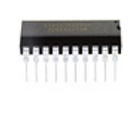
MC68HC908JK8CP Freescale Semiconductor, MC68HC908JK8CP Datasheet - Page 35

MC68HC908JK8CP
Manufacturer Part Number
MC68HC908JK8CP
Description
Manufacturer
Freescale Semiconductor
Datasheet
1.MC68HC908JK8CP.pdf
(212 pages)
Specifications of MC68HC908JK8CP
Cpu Family
HC08
Device Core Size
8b
Frequency (max)
8MHz
Interface Type
SCI
Program Memory Type
Flash
Program Memory Size
8KB
Total Internal Ram Size
256Byte
# I/os (max)
15
Number Of Timers - General Purpose
4
Operating Supply Voltage (typ)
3.3/5V
Operating Supply Voltage (max)
5.5V
Operating Supply Voltage (min)
2.7V
On-chip Adc
13-chx8-bit
Instruction Set Architecture
CISC
Operating Temp Range
-40C to 85C
Operating Temperature Classification
Industrial
Mounting
Through Hole
Pin Count
20
Package Type
PDIP
Lead Free Status / Rohs Status
Not Compliant
Available stocks
Company
Part Number
Manufacturer
Quantity
Price
Company:
Part Number:
MC68HC908JK8CP
Manufacturer:
ALTERA
Quantity:
13
Company:
Part Number:
MC68HC908JK8CPE
Manufacturer:
FREESCALE
Quantity:
928
Part Number:
MC68HC908JK8CPE
Manufacturer:
FREESCALE
Quantity:
20 000
- Current page: 35 of 212
- Download datasheet (2Mb)
2.9 FLASH Mass Erase Operation
Use the following procedure to erase the entire FLASH memory:
2.10 FLASH Program Operation
Programming of the FLASH memory is done on a row basis. A row consists of 32 consecutive bytes
starting from addresses $XX00, $XX20, $XX40, $XX60, $XX80, $XXA0, $XXC0 or $XXE0. Use this
step-by-step procedure to program a row of FLASH memory:
(Figure 2-4
Freescale Semiconductor
10. After time, t
10. After time, t
7. Clear the ERASE bit.
8. Wait for a time, t
9. Clear the HVEN bit.
1. Set both the ERASE bit and the MASS bit in the FLASH control register.
2. Read the FLASH block protect register.
3. Write any data to any FLASH location within the FLASH memory address range.
4. Wait for a time, t
5. Set the HVEN bit.
6. Wait for a time t
7. Clear the ERASE bit.
8. Wait for a time, t
9. Clear the HVEN bit.
1. Set the PGM bit. This configures the memory for program operation and enables the latching of
2. Read the FLASH block protect register.
3. Write any data to any FLASH location within the address range of the row to be programmed.
4. Wait for a time, t
5. Set the HVEN bit.
6. Wait for a time, t
7. Write data to the FLASH address to be programmed.
address and data for programming.
shows a flowchart of the programming algorithm.)
Programming and erasing of FLASH locations cannot be performed by
code being executed from the FLASH memory. While these operations
must be performed in the order as shown, but other unrelated operations
may occur between the steps.
Programming and erasing of FLASH locations cannot be performed by
code being executed from the FLASH memory. While these operations
must be performed in the order as shown, but other unrelated operations
may occur between the steps.
MC68HC908JL8/JK8 • MC68HC08JL8/JK8 • MC68HC908KL8 Data Sheet, Rev. 3.1
rcv
rcv
(1µs)
(1µs)
merase
nvh
nvs
nvh1
nvs
pgs
,
(10µs).
,
(10µs).
(5µs).
(5µs).
the memory can be accessed in read mode again.
the memory can be accessed in read mode again.
(100µs).
(4ms).
NOTE
NOTE
FLASH Mass Erase Operation
35
Related parts for MC68HC908JK8CP
Image
Part Number
Description
Manufacturer
Datasheet
Request
R
Part Number:
Description:
Manufacturer:
Freescale Semiconductor, Inc
Datasheet:
Part Number:
Description:
Manufacturer:
Freescale Semiconductor, Inc
Datasheet:
Part Number:
Description:
Manufacturer:
Freescale Semiconductor, Inc
Datasheet:
Part Number:
Description:
Manufacturer:
Freescale Semiconductor, Inc
Datasheet:
Part Number:
Description:
Manufacturer:
Freescale Semiconductor, Inc
Datasheet:
Part Number:
Description:
Manufacturer:
Freescale Semiconductor, Inc
Datasheet:
Part Number:
Description:
Manufacturer:
Freescale Semiconductor, Inc
Datasheet:
Part Number:
Description:
Manufacturer:
Freescale Semiconductor, Inc
Datasheet:
Part Number:
Description:
Manufacturer:
Freescale Semiconductor, Inc
Datasheet:
Part Number:
Description:
Manufacturer:
Freescale Semiconductor, Inc
Datasheet:
Part Number:
Description:
Manufacturer:
Freescale Semiconductor, Inc
Datasheet:
Part Number:
Description:
Manufacturer:
Freescale Semiconductor, Inc
Datasheet:
Part Number:
Description:
Manufacturer:
Freescale Semiconductor, Inc
Datasheet:
Part Number:
Description:
Manufacturer:
Freescale Semiconductor, Inc
Datasheet:
Part Number:
Description:
Manufacturer:
Freescale Semiconductor, Inc
Datasheet:


