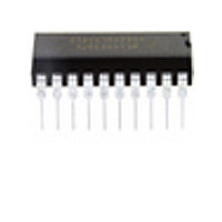
MC68HC908JK8CP Freescale Semiconductor, MC68HC908JK8CP Datasheet - Page 126

MC68HC908JK8CP
Manufacturer Part Number
MC68HC908JK8CP
Description
Manufacturer
Freescale Semiconductor
Datasheet
1.MC68HC908JK8CP.pdf
(212 pages)
Specifications of MC68HC908JK8CP
Cpu Family
HC08
Device Core Size
8b
Frequency (max)
8MHz
Interface Type
SCI
Program Memory Type
Flash
Program Memory Size
8KB
Total Internal Ram Size
256Byte
# I/os (max)
15
Number Of Timers - General Purpose
4
Operating Supply Voltage (typ)
3.3/5V
Operating Supply Voltage (max)
5.5V
Operating Supply Voltage (min)
2.7V
On-chip Adc
13-chx8-bit
Instruction Set Architecture
CISC
Operating Temp Range
-40C to 85C
Operating Temperature Classification
Industrial
Mounting
Through Hole
Pin Count
20
Package Type
PDIP
Lead Free Status / Rohs Status
Not Compliant
Available stocks
Company
Part Number
Manufacturer
Quantity
Price
Company:
Part Number:
MC68HC908JK8CP
Manufacturer:
ALTERA
Quantity:
13
Company:
Part Number:
MC68HC908JK8CPE
Manufacturer:
FREESCALE
Quantity:
928
Part Number:
MC68HC908JK8CPE
Manufacturer:
FREESCALE
Quantity:
20 000
- Current page: 126 of 212
- Download datasheet (2Mb)
Serial Communications Interface (SCI)
9.4.2.5 Inversion of Transmitted Output
The transmit inversion bit (TXINV) in SCI control register 1 (SCC1) reverses the polarity of transmitted
data. All transmitted values, including idle, break, start, and stop bits, are inverted when TXINV is at logic
1. (See
9.4.2.6 Transmitter Interrupts
These conditions can generate CPU interrupt requests from the SCI transmitter:
9.4.3 Receiver
Figure 9-5
9.4.3.1 Character Length
The receiver can accommodate either 8-bit or 9-bit data. The state of the M bit in SCI control register 1
(SCC1) determines character length. When receiving 9-bit data, bit R8 in SCI control register 2 (SCC2)
is the ninth bit (bit 8). When receiving 8-bit data, bit R8 is a copy of the eighth bit (bit 7).
9.4.3.2 Character Reception
During an SCI reception, the receive shift register shifts characters in from the RxD pin. The SCI data
register (SCDR) is the read-only buffer between the internal data bus and the receive shift register.
After a complete character shifts into the receive shift register, the data portion of the character transfers
to the SCDR. The SCI receiver full bit, SCRF, in SCI status register 1 (SCS1) becomes set, indicating that
the received byte can be read. If the SCI receive interrupt enable bit, SCRIE, in SCC2 is also set, the
SCRF bit generates a receiver CPU interrupt request.
126
•
•
SCI transmitter empty (SCTE) — The SCTE bit in SCS1 indicates that the SCDR has transferred
a character to the transmit shift register. SCTE can generate a transmitter CPU interrupt request.
Setting the SCI transmit interrupt enable bit, SCTIE, in SCC2 enables the SCTE bit to generate
transmitter CPU interrupt requests.
Transmission complete (TC) — The TC bit in SCS1 indicates that the transmit shift register and the
SCDR are empty and that no break or idle character has been generated. The transmission
complete interrupt enable bit, TCIE, in SCC2 enables the TC bit to generate transmitter CPU
interrupt requests.
9.8.1 SCI Control Register
shows the structure of the SCI receiver.
When queueing an idle character, return the TE bit to logic 1 before the stop
bit of the current character shifts out to the TxD pin. Setting TE after the stop
bit appears on TxD causes data previously written to the SCDR to be lost.
Toggle the TE bit for a queued idle character when the SCTE bit becomes
set and just before writing the next byte to the SCDR.
MC68HC908JL8/JK8 • MC68HC08JL8/JK8 • MC68HC908KL8 Data Sheet, Rev. 3.1
1.)
NOTE
Freescale Semiconductor
Related parts for MC68HC908JK8CP
Image
Part Number
Description
Manufacturer
Datasheet
Request
R
Part Number:
Description:
Manufacturer:
Freescale Semiconductor, Inc
Datasheet:
Part Number:
Description:
Manufacturer:
Freescale Semiconductor, Inc
Datasheet:
Part Number:
Description:
Manufacturer:
Freescale Semiconductor, Inc
Datasheet:
Part Number:
Description:
Manufacturer:
Freescale Semiconductor, Inc
Datasheet:
Part Number:
Description:
Manufacturer:
Freescale Semiconductor, Inc
Datasheet:
Part Number:
Description:
Manufacturer:
Freescale Semiconductor, Inc
Datasheet:
Part Number:
Description:
Manufacturer:
Freescale Semiconductor, Inc
Datasheet:
Part Number:
Description:
Manufacturer:
Freescale Semiconductor, Inc
Datasheet:
Part Number:
Description:
Manufacturer:
Freescale Semiconductor, Inc
Datasheet:
Part Number:
Description:
Manufacturer:
Freescale Semiconductor, Inc
Datasheet:
Part Number:
Description:
Manufacturer:
Freescale Semiconductor, Inc
Datasheet:
Part Number:
Description:
Manufacturer:
Freescale Semiconductor, Inc
Datasheet:
Part Number:
Description:
Manufacturer:
Freescale Semiconductor, Inc
Datasheet:
Part Number:
Description:
Manufacturer:
Freescale Semiconductor, Inc
Datasheet:
Part Number:
Description:
Manufacturer:
Freescale Semiconductor, Inc
Datasheet:


