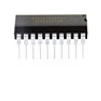
MC68HC908JK8CP Freescale Semiconductor, MC68HC908JK8CP Datasheet - Page 113

MC68HC908JK8CP
Manufacturer Part Number
MC68HC908JK8CP
Description
Manufacturer
Freescale Semiconductor
Datasheet
1.MC68HC908JK8CP.pdf
(212 pages)
Specifications of MC68HC908JK8CP
Cpu Family
HC08
Device Core Size
8b
Frequency (max)
8MHz
Interface Type
SCI
Program Memory Type
Flash
Program Memory Size
8KB
Total Internal Ram Size
256Byte
# I/os (max)
15
Number Of Timers - General Purpose
4
Operating Supply Voltage (typ)
3.3/5V
Operating Supply Voltage (max)
5.5V
Operating Supply Voltage (min)
2.7V
On-chip Adc
13-chx8-bit
Instruction Set Architecture
CISC
Operating Temp Range
-40C to 85C
Operating Temperature Classification
Industrial
Mounting
Through Hole
Pin Count
20
Package Type
PDIP
Lead Free Status / Rohs Status
Not Compliant
Available stocks
Company
Part Number
Manufacturer
Quantity
Price
Company:
Part Number:
MC68HC908JK8CP
Manufacturer:
ALTERA
Quantity:
13
Company:
Part Number:
MC68HC908JK8CPE
Manufacturer:
FREESCALE
Quantity:
928
Part Number:
MC68HC908JK8CPE
Manufacturer:
FREESCALE
Quantity:
20 000
- Current page: 113 of 212
- Download datasheet (2Mb)
8.7 TIM During Break Interrupts
A break interrupt stops the TIM counter.
The system integration module (SIM) controls whether status bits in other modules can be cleared during
the break state. The BCFE bit in the break flag control register (BFCR) enables software to clear status
bits during the break state. (See
To allow software to clear status bits during a break interrupt, write a logic 1 to the BCFE bit. If a status
bit is cleared during the break state, it remains cleared when the MCU exits the break state.
To protect status bits during the break state, write a logic 0 to the BCFE bit. With BCFE at logic 0 (its
default state), software can read and write I/O registers during the break state without affecting status bits.
Some status bits have a 2-step read/write clearing procedure. If software does the first step on such a bit
before the break, the bit cannot change during the break state as long as BCFE is at logic 0. After the
break, doing the second step clears the status bit.
8.8 I/O Signals
Port D shares two of its pins with TIM1 and port E shares two of its pins with TIM2. The ADC12/T2CLK
pin is an external clock input to TIM2. The four TIM channel I/O pins are T1CH0, T1CH1, T2CH0, and
T2CH1.
8.8.1 TIM Clock Pin (ADC12/T2CLK)
ADC12/T2CLK is an external clock input that can be the clock source for the TIM2 counter instead of the
prescaled internal bus clock. Select the ADC12/T2CLK input by writing logic 1’s to the three prescaler
select bits, PS[2:0]. (See
T2CLK
The maximum T2CLK frequency is:
ADC12/T2CLK is available as a ADC input channel pin when not used as the TIM2 clock input.
8.8.2 TIM Channel I/O Pins (PTD4/T1CH0, PTD5/T1CH1, PTE0/T2CH0, PTE1/T2CH1)
Each channel I/O pin is programmable independently as an input capture pin or an output compare pin.
T1CH0 and T2CH0 can be configured as buffered output compare or buffered PWM pins.
Freescale Semiconductor
LMIN
or T2CLK
MC68HC908JL8/JK8 • MC68HC08JL8/JK8 • MC68HC908KL8 Data Sheet, Rev. 3.1
HMIN
, is:
8.9.1 TIM Status and Control
5.7.3 Break Flag Control Register
bus frequency ÷ 2
------------------------------------ -
bus frequency
1
Register.) The minimum T2CLK pulse width,
+
t
SU
(BFCR).)
TIM During Break Interrupts
113
Related parts for MC68HC908JK8CP
Image
Part Number
Description
Manufacturer
Datasheet
Request
R
Part Number:
Description:
Manufacturer:
Freescale Semiconductor, Inc
Datasheet:
Part Number:
Description:
Manufacturer:
Freescale Semiconductor, Inc
Datasheet:
Part Number:
Description:
Manufacturer:
Freescale Semiconductor, Inc
Datasheet:
Part Number:
Description:
Manufacturer:
Freescale Semiconductor, Inc
Datasheet:
Part Number:
Description:
Manufacturer:
Freescale Semiconductor, Inc
Datasheet:
Part Number:
Description:
Manufacturer:
Freescale Semiconductor, Inc
Datasheet:
Part Number:
Description:
Manufacturer:
Freescale Semiconductor, Inc
Datasheet:
Part Number:
Description:
Manufacturer:
Freescale Semiconductor, Inc
Datasheet:
Part Number:
Description:
Manufacturer:
Freescale Semiconductor, Inc
Datasheet:
Part Number:
Description:
Manufacturer:
Freescale Semiconductor, Inc
Datasheet:
Part Number:
Description:
Manufacturer:
Freescale Semiconductor, Inc
Datasheet:
Part Number:
Description:
Manufacturer:
Freescale Semiconductor, Inc
Datasheet:
Part Number:
Description:
Manufacturer:
Freescale Semiconductor, Inc
Datasheet:
Part Number:
Description:
Manufacturer:
Freescale Semiconductor, Inc
Datasheet:
Part Number:
Description:
Manufacturer:
Freescale Semiconductor, Inc
Datasheet:


