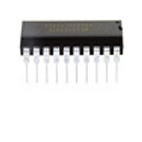
MC68HC908JK8CP Freescale Semiconductor, MC68HC908JK8CP Datasheet - Page 169

MC68HC908JK8CP
Manufacturer Part Number
MC68HC908JK8CP
Description
Manufacturer
Freescale Semiconductor
Datasheet
1.MC68HC908JK8CP.pdf
(212 pages)
Specifications of MC68HC908JK8CP
Cpu Family
HC08
Device Core Size
8b
Frequency (max)
8MHz
Interface Type
SCI
Program Memory Type
Flash
Program Memory Size
8KB
Total Internal Ram Size
256Byte
# I/os (max)
15
Number Of Timers - General Purpose
4
Operating Supply Voltage (typ)
3.3/5V
Operating Supply Voltage (max)
5.5V
Operating Supply Voltage (min)
2.7V
On-chip Adc
13-chx8-bit
Instruction Set Architecture
CISC
Operating Temp Range
-40C to 85C
Operating Temperature Classification
Industrial
Mounting
Through Hole
Pin Count
20
Package Type
PDIP
Lead Free Status / Rohs Status
Not Compliant
Available stocks
Company
Part Number
Manufacturer
Quantity
Price
Company:
Part Number:
MC68HC908JK8CP
Manufacturer:
ALTERA
Quantity:
13
Company:
Part Number:
MC68HC908JK8CPE
Manufacturer:
FREESCALE
Quantity:
928
Part Number:
MC68HC908JK8CPE
Manufacturer:
FREESCALE
Quantity:
20 000
- Current page: 169 of 212
- Download datasheet (2Mb)
If the MODEK bit is clear, the keyboard interrupt pin is falling-edge-sensitive only. With MODEK clear, a
vector fetch or software clear immediately clears the keyboard interrupt request.
Reset clears the keyboard interrupt request and the MODEK bit, clearing the interrupt request even if a
keyboard interrupt pin stays at logic 0.
The keyboard flag bit (KEYF) in the keyboard status and control register can be used to see if a pending
interrupt exists. The KEYF bit is not affected by the keyboard interrupt mask bit (IMASKK) which makes
it useful in applications where polling is preferred.
To determine the logic level on a keyboard interrupt pin, disable the pull-up device, use the data direction
register to configure the pin as an input and then read the data register.
13.4.1 Keyboard Initialization
When a keyboard interrupt pin is enabled, it takes time for the internal pull-up to reach a logic 1. Therefore
a false interrupt can occur as soon as the pin is enabled.
To prevent a false interrupt on keyboard initialization:
An interrupt signal on an edge-triggered pin can be acknowledged immediately after enabling the pin. An
interrupt signal on an edge- and level-triggered interrupt pin must be acknowledged after a delay that
depends on the external load.
Another way to avoid a false interrupt:
13.5 Keyboard Interrupt Registers
Two registers control the operation of the keyboard interrupt module:
13.5.1 Keyboard Status and Control Register
Freescale Semiconductor
1. Mask keyboard interrupts by setting the IMASKK bit in the keyboard status and control register.
2. Enable the KBI pins by setting the appropriate KBIEx bits in the keyboard interrupt enable register.
3. Write to the ACKK bit in the keyboard status and control register to clear any false interrupts.
4. Clear the IMASKK bit.
1. Configure the keyboard pins as outputs by setting the appropriate DDRA bits in the data direction
2. Write logic 1’s to the appropriate port A data register bits.
3. Enable the KBI pins by setting the appropriate KBIEx bits in the keyboard interrupt enable register.
•
•
•
•
•
•
register A.
Keyboard status and control register
Keyboard interrupt enable register
Flags keyboard interrupt requests
Acknowledges keyboard interrupt requests
Masks keyboard interrupt requests
Controls keyboard interrupt triggering sensitivity
Setting a keyboard interrupt enable bit (KBIEx) forces the corresponding
keyboard interrupt pin to be an input, overriding the data direction register.
However, the data direction register bit must be a logic 0 for software to
read the pin.
MC68HC908JL8/JK8 • MC68HC08JL8/JK8 • MC68HC908KL8 Data Sheet, Rev. 3.1
NOTE
Keyboard Interrupt Registers
169
Related parts for MC68HC908JK8CP
Image
Part Number
Description
Manufacturer
Datasheet
Request
R
Part Number:
Description:
Manufacturer:
Freescale Semiconductor, Inc
Datasheet:
Part Number:
Description:
Manufacturer:
Freescale Semiconductor, Inc
Datasheet:
Part Number:
Description:
Manufacturer:
Freescale Semiconductor, Inc
Datasheet:
Part Number:
Description:
Manufacturer:
Freescale Semiconductor, Inc
Datasheet:
Part Number:
Description:
Manufacturer:
Freescale Semiconductor, Inc
Datasheet:
Part Number:
Description:
Manufacturer:
Freescale Semiconductor, Inc
Datasheet:
Part Number:
Description:
Manufacturer:
Freescale Semiconductor, Inc
Datasheet:
Part Number:
Description:
Manufacturer:
Freescale Semiconductor, Inc
Datasheet:
Part Number:
Description:
Manufacturer:
Freescale Semiconductor, Inc
Datasheet:
Part Number:
Description:
Manufacturer:
Freescale Semiconductor, Inc
Datasheet:
Part Number:
Description:
Manufacturer:
Freescale Semiconductor, Inc
Datasheet:
Part Number:
Description:
Manufacturer:
Freescale Semiconductor, Inc
Datasheet:
Part Number:
Description:
Manufacturer:
Freescale Semiconductor, Inc
Datasheet:
Part Number:
Description:
Manufacturer:
Freescale Semiconductor, Inc
Datasheet:
Part Number:
Description:
Manufacturer:
Freescale Semiconductor, Inc
Datasheet:


