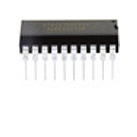
MC68HC908JK8CP Freescale Semiconductor, MC68HC908JK8CP Datasheet - Page 112

MC68HC908JK8CP
Manufacturer Part Number
MC68HC908JK8CP
Description
Manufacturer
Freescale Semiconductor
Datasheet
1.MC68HC908JK8CP.pdf
(212 pages)
Specifications of MC68HC908JK8CP
Cpu Family
HC08
Device Core Size
8b
Frequency (max)
8MHz
Interface Type
SCI
Program Memory Type
Flash
Program Memory Size
8KB
Total Internal Ram Size
256Byte
# I/os (max)
15
Number Of Timers - General Purpose
4
Operating Supply Voltage (typ)
3.3/5V
Operating Supply Voltage (max)
5.5V
Operating Supply Voltage (min)
2.7V
On-chip Adc
13-chx8-bit
Instruction Set Architecture
CISC
Operating Temp Range
-40C to 85C
Operating Temperature Classification
Industrial
Mounting
Through Hole
Pin Count
20
Package Type
PDIP
Lead Free Status / Rohs Status
Not Compliant
Available stocks
Company
Part Number
Manufacturer
Quantity
Price
Company:
Part Number:
MC68HC908JK8CP
Manufacturer:
ALTERA
Quantity:
13
Company:
Part Number:
MC68HC908JK8CPE
Manufacturer:
FREESCALE
Quantity:
928
Part Number:
MC68HC908JK8CPE
Manufacturer:
FREESCALE
Quantity:
20 000
- Current page: 112 of 212
- Download datasheet (2Mb)
Timer Interface Module (TIM)
Setting MS0B links channels 0 and 1 and configures them for buffered PWM operation. The TIM channel
0 registers (TCH0H:TCH0L) initially control the buffered PWM output. TIM status control register 0
(TSCR0) controls and monitors the PWM signal from the linked channels.
Clearing the toggle-on-overflow bit, TOVx, inhibits output toggles on TIM overflows. Subsequent output
compares try to force the output to a state it is already in and have no effect. The result is a 0% duty cycle
output.
Setting the channel x maximum duty cycle bit (CHxMAX) and setting the TOVx bit generates a 100% duty
cycle output. (See
8.5 Interrupts
The following TIM sources can generate interrupt requests:
8.6 Low-Power Modes
The WAIT and STOP instructions put the MCU in low power- consumption standby modes.
8.6.1 Wait Mode
The TIM remains active after the execution of a WAIT instruction. In wait mode, the TIM registers are not
accessible by the CPU. Any enabled CPU interrupt request from the TIM can bring the MCU out of wait
mode.
If TIM functions are not required during wait mode, reduce power consumption by stopping the TIM before
executing the WAIT instruction.
8.6.2 Stop Mode
The TIM is inactive after the execution of a STOP instruction. The STOP instruction does not affect
register conditions or the state of the TIM counter. TIM operation resumes when the MCU exits stop mode
after an external interrupt.
112
5. In the TIM status control register (TSC), clear the TIM stop bit, TSTOP.
•
•
TIM overflow flag (TOF) — The TOF bit is set when the TIM counter reaches the modulo value
programmed in the TIM counter modulo registers. The TIM overflow interrupt enable bit, TOIE,
enables TIM overflow CPU interrupt requests. TOF and TOIE are in the TIM status and control
register.
TIM channel flags (CH1F:CH0F) — The CHxF bit is set when an input capture or output compare
occurs on channel x. Channel x TIM CPU interrupt requests are controlled by the channel x
interrupt enable bit, CHxIE. Channel x TIM CPU interrupt requests are enabled when CHxIE = 1.
CHxF and CHxIE are in the TIM channel x status and control register.
cycle generation and removes the ability of the channel to self-correct in the
event of software error or noise. Toggling on output compare can also
cause incorrect PWM signal generation when changing the PWM pulse
width to a new, much larger value.
MC68HC908JL8/JK8 • MC68HC08JL8/JK8 • MC68HC908KL8 Data Sheet, Rev. 3.1
8.9.4 TIM Channel Status and Control
Registers.)
Freescale Semiconductor
Related parts for MC68HC908JK8CP
Image
Part Number
Description
Manufacturer
Datasheet
Request
R
Part Number:
Description:
Manufacturer:
Freescale Semiconductor, Inc
Datasheet:
Part Number:
Description:
Manufacturer:
Freescale Semiconductor, Inc
Datasheet:
Part Number:
Description:
Manufacturer:
Freescale Semiconductor, Inc
Datasheet:
Part Number:
Description:
Manufacturer:
Freescale Semiconductor, Inc
Datasheet:
Part Number:
Description:
Manufacturer:
Freescale Semiconductor, Inc
Datasheet:
Part Number:
Description:
Manufacturer:
Freescale Semiconductor, Inc
Datasheet:
Part Number:
Description:
Manufacturer:
Freescale Semiconductor, Inc
Datasheet:
Part Number:
Description:
Manufacturer:
Freescale Semiconductor, Inc
Datasheet:
Part Number:
Description:
Manufacturer:
Freescale Semiconductor, Inc
Datasheet:
Part Number:
Description:
Manufacturer:
Freescale Semiconductor, Inc
Datasheet:
Part Number:
Description:
Manufacturer:
Freescale Semiconductor, Inc
Datasheet:
Part Number:
Description:
Manufacturer:
Freescale Semiconductor, Inc
Datasheet:
Part Number:
Description:
Manufacturer:
Freescale Semiconductor, Inc
Datasheet:
Part Number:
Description:
Manufacturer:
Freescale Semiconductor, Inc
Datasheet:
Part Number:
Description:
Manufacturer:
Freescale Semiconductor, Inc
Datasheet:


