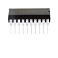
MC68HC908JK8CP Freescale Semiconductor, MC68HC908JK8CP Datasheet - Page 154

MC68HC908JK8CP
Manufacturer Part Number
MC68HC908JK8CP
Description
Manufacturer
Freescale Semiconductor
Datasheet
1.MC68HC908JK8CP.pdf
(212 pages)
Specifications of MC68HC908JK8CP
Cpu Family
HC08
Device Core Size
8b
Frequency (max)
8MHz
Interface Type
SCI
Program Memory Type
Flash
Program Memory Size
8KB
Total Internal Ram Size
256Byte
# I/os (max)
15
Number Of Timers - General Purpose
4
Operating Supply Voltage (typ)
3.3/5V
Operating Supply Voltage (max)
5.5V
Operating Supply Voltage (min)
2.7V
On-chip Adc
13-chx8-bit
Instruction Set Architecture
CISC
Operating Temp Range
-40C to 85C
Operating Temperature Classification
Industrial
Mounting
Through Hole
Pin Count
20
Package Type
PDIP
Lead Free Status / Rohs Status
Not Compliant
Available stocks
Company
Part Number
Manufacturer
Quantity
Price
Company:
Part Number:
MC68HC908JK8CP
Manufacturer:
ALTERA
Quantity:
13
Company:
Part Number:
MC68HC908JK8CPE
Manufacturer:
FREESCALE
Quantity:
928
Part Number:
MC68HC908JK8CPE
Manufacturer:
FREESCALE
Quantity:
20 000
- Current page: 154 of 212
- Download datasheet (2Mb)
Input/Output (I/O) Ports
DDRA[7:0] — Data Direction Register A Bits
Figure 11-4
When DDRAx is a logic 1, reading address $0000 reads the PTAx data latch. When DDRAx is a logic 0,
reading address $0000 reads the voltage level on the pin. The data latch can always be written,
regardless of the state of its data direction bit.
Table 11-2
154
These read/write bits control port A data direction. Reset clears DDRA[7:0], configuring all port A pins
as inputs.
1 = Corresponding port A pin configured as output
0 = Corresponding port A pin configured as input
PTAPUE
1. X = Don’t care.
2. Pin pulled to V
3. Writing affects data register, but does not affect input.
4. Hi-Z = High impedance.
summarizes the operation of the port A pins.
Bit
shows the port A I/O logic.
X
1
0
Address:
Avoid glitches on port A pins by writing to the port A data register before
changing data direction register A bits from 0 to 1.
Reset:
Read:
Write:
MC68HC908JL8/JK8 • MC68HC08JL8/JK8 • MC68HC908KL8 Data Sheet, Rev. 3.1
DDRA Bit
READ DDRA ($0004)
WRITE DDRA ($0004)
WRITE PTA ($0000)
READ PTA ($0000)
DDRA7
0
0
1
$0004
DD
Bit 7
0
by internal pull-up.
Figure 11-3. Data Direction Register A (DDRA)
PTA Bit
DDRA6
X
X
X
(1)
6
0
Table 11-2. Port A Pin Functions
RESET
Figure 11-4. Port A I/O Circuit
I/O Pin Mode
Input, Hi-Z
DDRA5
Input, V
5
0
Output
DD
NOTE
(2)
(4)
DDRA4
DDRAx
PTAx
4
0
Accesses to DDRA
Read/Write
DDRA3
DDRA[7:0]
DDRA[7:0]
DDRA[7:0]
3
0
DDRA2
2
0
PTAPUEx
PTA[7:0]
DDRA1
Read
Pin
Pin
Accesses to PTA
1
0
To KBI
Freescale Semiconductor
DDRA0
PTA[7:0]
PTA[7:0]
Bit 0
PTA[7:0]
PTAx
0
Write
(3)
(3)
Related parts for MC68HC908JK8CP
Image
Part Number
Description
Manufacturer
Datasheet
Request
R
Part Number:
Description:
Manufacturer:
Freescale Semiconductor, Inc
Datasheet:
Part Number:
Description:
Manufacturer:
Freescale Semiconductor, Inc
Datasheet:
Part Number:
Description:
Manufacturer:
Freescale Semiconductor, Inc
Datasheet:
Part Number:
Description:
Manufacturer:
Freescale Semiconductor, Inc
Datasheet:
Part Number:
Description:
Manufacturer:
Freescale Semiconductor, Inc
Datasheet:
Part Number:
Description:
Manufacturer:
Freescale Semiconductor, Inc
Datasheet:
Part Number:
Description:
Manufacturer:
Freescale Semiconductor, Inc
Datasheet:
Part Number:
Description:
Manufacturer:
Freescale Semiconductor, Inc
Datasheet:
Part Number:
Description:
Manufacturer:
Freescale Semiconductor, Inc
Datasheet:
Part Number:
Description:
Manufacturer:
Freescale Semiconductor, Inc
Datasheet:
Part Number:
Description:
Manufacturer:
Freescale Semiconductor, Inc
Datasheet:
Part Number:
Description:
Manufacturer:
Freescale Semiconductor, Inc
Datasheet:
Part Number:
Description:
Manufacturer:
Freescale Semiconductor, Inc
Datasheet:
Part Number:
Description:
Manufacturer:
Freescale Semiconductor, Inc
Datasheet:
Part Number:
Description:
Manufacturer:
Freescale Semiconductor, Inc
Datasheet:


