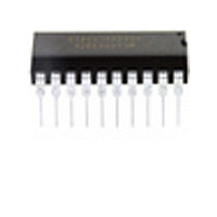
MC68HC908JK8CP Freescale Semiconductor, MC68HC908JK8CP Datasheet - Page 87

MC68HC908JK8CP
Manufacturer Part Number
MC68HC908JK8CP
Description
Manufacturer
Freescale Semiconductor
Datasheet
1.MC68HC908JK8CP.pdf
(212 pages)
Specifications of MC68HC908JK8CP
Cpu Family
HC08
Device Core Size
8b
Frequency (max)
8MHz
Interface Type
SCI
Program Memory Type
Flash
Program Memory Size
8KB
Total Internal Ram Size
256Byte
# I/os (max)
15
Number Of Timers - General Purpose
4
Operating Supply Voltage (typ)
3.3/5V
Operating Supply Voltage (max)
5.5V
Operating Supply Voltage (min)
2.7V
On-chip Adc
13-chx8-bit
Instruction Set Architecture
CISC
Operating Temp Range
-40C to 85C
Operating Temperature Classification
Industrial
Mounting
Through Hole
Pin Count
20
Package Type
PDIP
Lead Free Status / Rohs Status
Not Compliant
Available stocks
Company
Part Number
Manufacturer
Quantity
Price
Company:
Part Number:
MC68HC908JK8CP
Manufacturer:
ALTERA
Quantity:
13
Company:
Part Number:
MC68HC908JK8CPE
Manufacturer:
FREESCALE
Quantity:
928
Part Number:
MC68HC908JK8CPE
Manufacturer:
FREESCALE
Quantity:
20 000
- Current page: 87 of 212
- Download datasheet (2Mb)
7.3.1 Entering Monitor Mode
Table 7-1
may be entered after a POR.
Communication at 9600 baud will be established provided one of the following sets of conditions is met:
If V
frequency is a divide-by-two of the clock input to OSC1. If PTB3 is high with V
monitor mode entry
OSC1. Holding the PTB3 pin low when entering monitor mode causes a bypass of a divide-by-two stage
at the oscillator only if V
2OSCOUT frequency, and OSC1 input directly generates internal bus clocks. In this case, the OSC1
signal must have a 50% duty cycle at maximum bus frequency.
Entering monitor mode with V
RST. (See
If entering monitor mode without high voltage on IRQ and reset vector being blank ($FFFE and $FFFF)
(Table 7-1
Freescale Semiconductor
1. RC oscillator cannot be used for monitor mode; must use either external oscillator or XTAL oscillator circuit.
2. See
1. If IRQ = V
2. If IRQ = V
3. If $FFFE and $FFFF are blank (contain $FF):
V
V
TST
TST
TST
V
V
IRQ
DD
DD
–
–
–
–
–
–
(2)
(1)
Table 17-4
is applied to IRQ and PTB3 is low upon monitor mode entry
shows the pin conditions for entering monitor mode. As specified in the table, monitor mode
Clock on OSC1 is 4.9125MHz
PTB3 = low
Clock on OSC1 is 9.8304MHz
PTB3 = high
Clock on OSC1 is 9.8304MHz
IRQ = V
condition set 3, where applied voltage is V
Chapter 5 System Integration Module (SIM)
(contain
BLANK
BLANK
$FFFE
$FFFF
$FF)
NOT
and
TST
TST
for V
X
X
MC68HC908JL8/JK8 • MC68HC08JL8/JK8 • MC68HC908KL8 Data Sheet, Rev. 3.1
DD
(Table 7-1
:
:
TST
Table 7-1. Monitor Mode Entry Requirements and Options
TST
voltage level requirements.
X
X
0
1
is applied to IRQ. In this event, the OSCOUT frequency is equal to the
0
0
X
X
TST
condition set 2), the bus frequency is a divide-by-four of the clock input to
on IRQ, the COP is disabled as long as V
X
X
1
1
X
1
1
1
OSC1 Clock
4.9152MHz
9.8304MHz
9.8304MHz
X
DD
(1)
), then all port B pin requirements and conditions,
for more information on modes of operation.)
Bus Frequency
2.4576MHz
2.4576MHz
2.4576MHz
OSC1 ÷ 4
(Table 7-1
TST
TST
is applied to either IRQ or
High voltage entry to monitor
mode.
9600 baud communication on
PTB0. COP disabled.
Blank reset vector
(low-voltage) entry to monitor
mode.
9600 baud communication on
PTB0. COP disabled.
Enters User mode.
condition set 1), the bus
applied to IRQ upon
Functional Description
Comments
87
Related parts for MC68HC908JK8CP
Image
Part Number
Description
Manufacturer
Datasheet
Request
R
Part Number:
Description:
Manufacturer:
Freescale Semiconductor, Inc
Datasheet:
Part Number:
Description:
Manufacturer:
Freescale Semiconductor, Inc
Datasheet:
Part Number:
Description:
Manufacturer:
Freescale Semiconductor, Inc
Datasheet:
Part Number:
Description:
Manufacturer:
Freescale Semiconductor, Inc
Datasheet:
Part Number:
Description:
Manufacturer:
Freescale Semiconductor, Inc
Datasheet:
Part Number:
Description:
Manufacturer:
Freescale Semiconductor, Inc
Datasheet:
Part Number:
Description:
Manufacturer:
Freescale Semiconductor, Inc
Datasheet:
Part Number:
Description:
Manufacturer:
Freescale Semiconductor, Inc
Datasheet:
Part Number:
Description:
Manufacturer:
Freescale Semiconductor, Inc
Datasheet:
Part Number:
Description:
Manufacturer:
Freescale Semiconductor, Inc
Datasheet:
Part Number:
Description:
Manufacturer:
Freescale Semiconductor, Inc
Datasheet:
Part Number:
Description:
Manufacturer:
Freescale Semiconductor, Inc
Datasheet:
Part Number:
Description:
Manufacturer:
Freescale Semiconductor, Inc
Datasheet:
Part Number:
Description:
Manufacturer:
Freescale Semiconductor, Inc
Datasheet:
Part Number:
Description:
Manufacturer:
Freescale Semiconductor, Inc
Datasheet:


