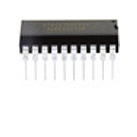
MC68HC908JK8CP Freescale Semiconductor, MC68HC908JK8CP Datasheet - Page 61

MC68HC908JK8CP
Manufacturer Part Number
MC68HC908JK8CP
Description
Manufacturer
Freescale Semiconductor
Datasheet
1.MC68HC908JK8CP.pdf
(212 pages)
Specifications of MC68HC908JK8CP
Cpu Family
HC08
Device Core Size
8b
Frequency (max)
8MHz
Interface Type
SCI
Program Memory Type
Flash
Program Memory Size
8KB
Total Internal Ram Size
256Byte
# I/os (max)
15
Number Of Timers - General Purpose
4
Operating Supply Voltage (typ)
3.3/5V
Operating Supply Voltage (max)
5.5V
Operating Supply Voltage (min)
2.7V
On-chip Adc
13-chx8-bit
Instruction Set Architecture
CISC
Operating Temp Range
-40C to 85C
Operating Temperature Classification
Industrial
Mounting
Through Hole
Pin Count
20
Package Type
PDIP
Lead Free Status / Rohs Status
Not Compliant
Available stocks
Company
Part Number
Manufacturer
Quantity
Price
Company:
Part Number:
MC68HC908JK8CP
Manufacturer:
ALTERA
Quantity:
13
Company:
Part Number:
MC68HC908JK8CPE
Manufacturer:
FREESCALE
Quantity:
928
Part Number:
MC68HC908JK8CPE
Manufacturer:
FREESCALE
Quantity:
20 000
- Current page: 61 of 212
- Download datasheet (2Mb)
Chapter 5
System Integration Module (SIM)
5.1 Introduction
This section describes the system integration module (SIM), which supports up to 24 external and/or
internal interrupts. Together with the CPU, the SIM controls all MCU activities. A block diagram of the SIM
is shown in
controller that coordinates CPU and exception timing.
The SIM is responsible for:
Table 5-1
Freescale Semiconductor
•
•
•
•
•
Bus clock generation and control for CPU and peripherals
–
–
Master reset control, including power-on reset (POR) and COP timeout
Interrupt control:
–
–
–
CPU enable/disable timing
Modular architecture expandable to 128 interrupt sources
Signal Name
shows the internal signal names used in this section.
Stop/wait/reset/break entry and recovery
Internal clock control
Acknowledge timing
Arbitration control timing
Vector address generation
OSCOUT
PORRST
Figure
ICLK
IRST
R/W
IAB
IDB
MC68HC908JL8/JK8 • MC68HC08JL8/JK8 • MC68HC908KL8 Data Sheet, Rev. 3.1
5-1.
Figure 5-2
Internal oscillator clock
The XTAL or RC frequency divided by two. This signal is again divided by two in the SIM
to generate the internal bus clocks. (Bus clock = OSCOUT ÷ 2)
Internal address bus
Internal data bus
Signal from the power-on reset module to the SIM
Internal reset signal
Read/write signal
Table 5-1. Signal Name Conventions
is a summary of the SIM I/O registers. The SIM is a system state
Description
61
Related parts for MC68HC908JK8CP
Image
Part Number
Description
Manufacturer
Datasheet
Request
R
Part Number:
Description:
Manufacturer:
Freescale Semiconductor, Inc
Datasheet:
Part Number:
Description:
Manufacturer:
Freescale Semiconductor, Inc
Datasheet:
Part Number:
Description:
Manufacturer:
Freescale Semiconductor, Inc
Datasheet:
Part Number:
Description:
Manufacturer:
Freescale Semiconductor, Inc
Datasheet:
Part Number:
Description:
Manufacturer:
Freescale Semiconductor, Inc
Datasheet:
Part Number:
Description:
Manufacturer:
Freescale Semiconductor, Inc
Datasheet:
Part Number:
Description:
Manufacturer:
Freescale Semiconductor, Inc
Datasheet:
Part Number:
Description:
Manufacturer:
Freescale Semiconductor, Inc
Datasheet:
Part Number:
Description:
Manufacturer:
Freescale Semiconductor, Inc
Datasheet:
Part Number:
Description:
Manufacturer:
Freescale Semiconductor, Inc
Datasheet:
Part Number:
Description:
Manufacturer:
Freescale Semiconductor, Inc
Datasheet:
Part Number:
Description:
Manufacturer:
Freescale Semiconductor, Inc
Datasheet:
Part Number:
Description:
Manufacturer:
Freescale Semiconductor, Inc
Datasheet:
Part Number:
Description:
Manufacturer:
Freescale Semiconductor, Inc
Datasheet:
Part Number:
Description:
Manufacturer:
Freescale Semiconductor, Inc
Datasheet:


