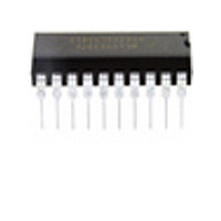
MC68HC908JK8CP Freescale Semiconductor, MC68HC908JK8CP Datasheet - Page 38

MC68HC908JK8CP
Manufacturer Part Number
MC68HC908JK8CP
Description
Manufacturer
Freescale Semiconductor
Datasheet
1.MC68HC908JK8CP.pdf
(212 pages)
Specifications of MC68HC908JK8CP
Cpu Family
HC08
Device Core Size
8b
Frequency (max)
8MHz
Interface Type
SCI
Program Memory Type
Flash
Program Memory Size
8KB
Total Internal Ram Size
256Byte
# I/os (max)
15
Number Of Timers - General Purpose
4
Operating Supply Voltage (typ)
3.3/5V
Operating Supply Voltage (max)
5.5V
Operating Supply Voltage (min)
2.7V
On-chip Adc
13-chx8-bit
Instruction Set Architecture
CISC
Operating Temp Range
-40C to 85C
Operating Temperature Classification
Industrial
Mounting
Through Hole
Pin Count
20
Package Type
PDIP
Lead Free Status / Rohs Status
Not Compliant
Available stocks
Company
Part Number
Manufacturer
Quantity
Price
Company:
Part Number:
MC68HC908JK8CP
Manufacturer:
ALTERA
Quantity:
13
Company:
Part Number:
MC68HC908JK8CPE
Manufacturer:
FREESCALE
Quantity:
928
Part Number:
MC68HC908JK8CPE
Manufacturer:
FREESCALE
Quantity:
20 000
- Current page: 38 of 212
- Download datasheet (2Mb)
Memory
2.11 FLASH Block Protection
Due to the ability of the on-board charge pump to erase and program the FLASH memory in the target
application, provision is made to protect blocks of memory from unintentional erase or program operations
due to system malfunction. This protection is done by use of a FLASH block protect register (FLBPR).
The FLBPR determines the range of the FLASH memory which is to be protected. The range of the
protected area starts from a location defined by FLBPR and ends to the bottom of the FLASH memory
($FFFF). When the memory is protected, the HVEN bit cannot be set in either erase or program
operations.
In performing a program or erase operation, the FLASH block protect register must be read after setting
the PGM or ERASE bit and before asserting the HVEN bit
When the FLBPR is program with all 0’s, the entire memory is protected from being programmed and
erased. When all the bits are erased
(all 1’s), the entire memory is accessible for program and erase.
When bits within the FLBPR are programmed, they lock a block of memory, address ranges as shown in
2.12 FLASH Block Protect
erase or program of the FLBPR or the protected block of FLASH memory is prohibited. The FLBPR itself
can be erased or programmed only with an external voltage, V
also allows entry from reset into the monitor mode.
2.12 FLASH Block Protect Register
The FLASH block protect register (FLBPR) is implemented as a byte within the FLASH memory, and
therefore can only be written during a programming sequence of the FLASH memory. The value in this
register determines the starting location of the protected range within the FLASH memory.
BPR[7:0] — FLASH Block Protect Bits
38
BPR[7:0] represent bits [13:6] of a 16-bit memory address. Bits [15:14] are logic 1’s and bits [5:0] are
logic 0’s.
Non-volatile FLASH register; write by programming.
Address:
Reset:
Read:
Write:
Start address of FLASH block protect
MC68HC908JL8/JK8 • MC68HC08JL8/JK8 • MC68HC908KL8 Data Sheet, Rev. 3.1
$FFCF
BPR7
Bit 7
Figure 2-5. FLASH Block Protect Register (FLBPR)
Register. Once the FLBPR is programmed with a value other than $FF, any
BPR6
6
BPR5
5
Unaffected by reset; $FF when blank
NOTE
BPR4
1 1
4
BPR3
3
16-bit memory address
BPR[7:0]
TST
, present on the IRQ pin. This voltage
BPR2
2
BPR1
0 0 0 0 0 0
1
Freescale Semiconductor
BPR0
Bit 0
Related parts for MC68HC908JK8CP
Image
Part Number
Description
Manufacturer
Datasheet
Request
R
Part Number:
Description:
Manufacturer:
Freescale Semiconductor, Inc
Datasheet:
Part Number:
Description:
Manufacturer:
Freescale Semiconductor, Inc
Datasheet:
Part Number:
Description:
Manufacturer:
Freescale Semiconductor, Inc
Datasheet:
Part Number:
Description:
Manufacturer:
Freescale Semiconductor, Inc
Datasheet:
Part Number:
Description:
Manufacturer:
Freescale Semiconductor, Inc
Datasheet:
Part Number:
Description:
Manufacturer:
Freescale Semiconductor, Inc
Datasheet:
Part Number:
Description:
Manufacturer:
Freescale Semiconductor, Inc
Datasheet:
Part Number:
Description:
Manufacturer:
Freescale Semiconductor, Inc
Datasheet:
Part Number:
Description:
Manufacturer:
Freescale Semiconductor, Inc
Datasheet:
Part Number:
Description:
Manufacturer:
Freescale Semiconductor, Inc
Datasheet:
Part Number:
Description:
Manufacturer:
Freescale Semiconductor, Inc
Datasheet:
Part Number:
Description:
Manufacturer:
Freescale Semiconductor, Inc
Datasheet:
Part Number:
Description:
Manufacturer:
Freescale Semiconductor, Inc
Datasheet:
Part Number:
Description:
Manufacturer:
Freescale Semiconductor, Inc
Datasheet:
Part Number:
Description:
Manufacturer:
Freescale Semiconductor, Inc
Datasheet:


