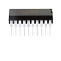
MC68HC908JK8CP Freescale Semiconductor, MC68HC908JK8CP Datasheet - Page 148

MC68HC908JK8CP
Manufacturer Part Number
MC68HC908JK8CP
Description
Manufacturer
Freescale Semiconductor
Datasheet
1.MC68HC908JK8CP.pdf
(212 pages)
Specifications of MC68HC908JK8CP
Cpu Family
HC08
Device Core Size
8b
Frequency (max)
8MHz
Interface Type
SCI
Program Memory Type
Flash
Program Memory Size
8KB
Total Internal Ram Size
256Byte
# I/os (max)
15
Number Of Timers - General Purpose
4
Operating Supply Voltage (typ)
3.3/5V
Operating Supply Voltage (max)
5.5V
Operating Supply Voltage (min)
2.7V
On-chip Adc
13-chx8-bit
Instruction Set Architecture
CISC
Operating Temp Range
-40C to 85C
Operating Temperature Classification
Industrial
Mounting
Through Hole
Pin Count
20
Package Type
PDIP
Lead Free Status / Rohs Status
Not Compliant
Available stocks
Company
Part Number
Manufacturer
Quantity
Price
Company:
Part Number:
MC68HC908JK8CP
Manufacturer:
ALTERA
Quantity:
13
Company:
Part Number:
MC68HC908JK8CPE
Manufacturer:
FREESCALE
Quantity:
928
Part Number:
MC68HC908JK8CPE
Manufacturer:
FREESCALE
Quantity:
20 000
- Current page: 148 of 212
- Download datasheet (2Mb)
Analog-to-Digital Converter (ADC)
10.5.2 Stop Mode
The ADC module is inactive after the execution of a STOP instruction. Any pending conversion is aborted.
ADC conversions resume when the MCU exits stop mode. Allow one conversion cycle to stabilize the
analog circuitry before attempting a new ADC conversion after exiting stop mode.
10.6 I/O Signals
The ADC module has 12 channels that are shared with I/O port B and port D, and one channel on
ADC12/T2CLK pin.
10.6.1 ADC Voltage In (ADCVIN)
ADCVIN is the input voltage signal from one of the 13 ADC channels to the ADC module.
10.7 I/O Registers
These I/O registers control and monitor ADC operation:
10.7.1 ADC Status and Control Register
The following paragraphs describe the function of the ADC status and control register.
COCO — Conversions Complete Bit
AIEN — ADC Interrupt Enable Bit
148
•
•
•
When the AIEN bit is a logic 0, the COCO is a read-only bit which is set each time a conversion is
completed. This bit is cleared whenever the ADC status and control register is written or whenever the
ADC data register is read. Reset clears this bit.
When the AIEN bit is a logic 1 (CPU interrupt enabled), the COCO is a read-only bit, and will always
be logic 0 when read.
When this bit is set, an interrupt is generated at the end of an ADC conversion. The interrupt signal is
cleared when the data register is read or the status/control register is written. Reset clears the AIEN bit.
1 = Conversion completed (AIEN = 0)
0 = Conversion not completed (AIEN = 0)
1 = ADC interrupt enabled
0 = ADC interrupt disabled
ADC status and control register (ADSCR)
ADC data register (ADR)
ADC clock register (ADICLK)
Address:
Reset:
Read:
Write:
MC68HC908JL8/JK8 • MC68HC08JL8/JK8 • MC68HC908KL8 Data Sheet, Rev. 3.1
Figure 10-3. ADC Status and Control Register (ADSCR)
$003C
COCO
Bit 7
0
AIEN
6
0
= Unimplemented
ADCO
5
0
ADCH4
4
1
ADCH3
3
1
ADCH2
2
1
ADCH1
1
1
Freescale Semiconductor
ADCH0
Bit 0
1
Related parts for MC68HC908JK8CP
Image
Part Number
Description
Manufacturer
Datasheet
Request
R
Part Number:
Description:
Manufacturer:
Freescale Semiconductor, Inc
Datasheet:
Part Number:
Description:
Manufacturer:
Freescale Semiconductor, Inc
Datasheet:
Part Number:
Description:
Manufacturer:
Freescale Semiconductor, Inc
Datasheet:
Part Number:
Description:
Manufacturer:
Freescale Semiconductor, Inc
Datasheet:
Part Number:
Description:
Manufacturer:
Freescale Semiconductor, Inc
Datasheet:
Part Number:
Description:
Manufacturer:
Freescale Semiconductor, Inc
Datasheet:
Part Number:
Description:
Manufacturer:
Freescale Semiconductor, Inc
Datasheet:
Part Number:
Description:
Manufacturer:
Freescale Semiconductor, Inc
Datasheet:
Part Number:
Description:
Manufacturer:
Freescale Semiconductor, Inc
Datasheet:
Part Number:
Description:
Manufacturer:
Freescale Semiconductor, Inc
Datasheet:
Part Number:
Description:
Manufacturer:
Freescale Semiconductor, Inc
Datasheet:
Part Number:
Description:
Manufacturer:
Freescale Semiconductor, Inc
Datasheet:
Part Number:
Description:
Manufacturer:
Freescale Semiconductor, Inc
Datasheet:
Part Number:
Description:
Manufacturer:
Freescale Semiconductor, Inc
Datasheet:
Part Number:
Description:
Manufacturer:
Freescale Semiconductor, Inc
Datasheet:


