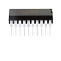
MC68HC908JK8CP Freescale Semiconductor, MC68HC908JK8CP Datasheet - Page 117

MC68HC908JK8CP
Manufacturer Part Number
MC68HC908JK8CP
Description
Manufacturer
Freescale Semiconductor
Datasheet
1.MC68HC908JK8CP.pdf
(212 pages)
Specifications of MC68HC908JK8CP
Cpu Family
HC08
Device Core Size
8b
Frequency (max)
8MHz
Interface Type
SCI
Program Memory Type
Flash
Program Memory Size
8KB
Total Internal Ram Size
256Byte
# I/os (max)
15
Number Of Timers - General Purpose
4
Operating Supply Voltage (typ)
3.3/5V
Operating Supply Voltage (max)
5.5V
Operating Supply Voltage (min)
2.7V
On-chip Adc
13-chx8-bit
Instruction Set Architecture
CISC
Operating Temp Range
-40C to 85C
Operating Temperature Classification
Industrial
Mounting
Through Hole
Pin Count
20
Package Type
PDIP
Lead Free Status / Rohs Status
Not Compliant
Available stocks
Company
Part Number
Manufacturer
Quantity
Price
Company:
Part Number:
MC68HC908JK8CP
Manufacturer:
ALTERA
Quantity:
13
Company:
Part Number:
MC68HC908JK8CPE
Manufacturer:
FREESCALE
Quantity:
928
Part Number:
MC68HC908JK8CPE
Manufacturer:
FREESCALE
Quantity:
20 000
- Current page: 117 of 212
- Download datasheet (2Mb)
8.9.4 TIM Channel Status and Control Registers
Each of the TIM channel status and control registers:
CHxF — Channel x Flag Bit
CHxIE — Channel x Interrupt Enable Bit
MSxB — Mode Select Bit B
Freescale Semiconductor
•
•
•
•
•
•
•
•
When channel x is an input capture channel, this read/write bit is set when an active edge occurs on
the channel x pin. When channel x is an output compare channel, CHxF is set when the value in the
TIM counter registers matches the value in the TIM channel x registers.
When TIM CPU interrupt requests are enabled (CHxIE = 1), clear CHxF by reading TIM channel x
status and control register with CHxF set and then writing a logic 0 to CHxF. If another interrupt request
occurs before the clearing sequence is complete, then writing logic 0 to CHxF has no effect. Therefore,
an interrupt request cannot be lost due to inadvertent clearing of CHxF.
Reset clears the CHxF bit. Writing a logic 1 to CHxF has no effect.
This read/write bit enables TIM CPU interrupt service requests on channel x.
Reset clears the CHxIE bit.
This read/write bit selects buffered output compare/PWM operation. MSxB exists only in the TIM1
channel 0 and TIM2 channel 0 status and control registers.
1 = Input capture or output compare on channel x
0 = No input capture or output compare on channel x
1 = Channel x CPU interrupt requests enabled
0 = Channel x CPU interrupt requests disabled
Flags input captures and output compares
Enables input capture and output compare interrupts
Selects input capture, output compare, or PWM operation
Selects high, low, or toggling output on output compare
Selects rising edge, falling edge, or any edge as the active input capture trigger
Selects output toggling on TIM overflow
Selects 0% and 100% PWM duty cycle
Selects buffered or unbuffered output compare/PWM operation
Address: T1SC0, $0025 and T2SC0, $0035
Address: T1SC1, $0028 and T2SC1, $0038
Reset:
Reset:
Read:
Read:
Write:
Write:
MC68HC908JL8/JK8 • MC68HC08JL8/JK8 • MC68HC908KL8 Data Sheet, Rev. 3.1
Figure 8-10. TIM Channel 1 Status and Control Register (TSC1)
Figure 8-9. TIM Channel 0 Status and Control Register (TSC0)
CH0F
CH1F
Bit 7
Bit 7
0
0
0
0
CH0IE
CH1IE
6
0
6
0
MS0B
5
0
5
0
0
MS0A
MS1A
4
0
4
0
ELS0B
ELS1B
3
0
3
0
ELS0A
ELS1A
2
0
2
0
TOV0
TOV1
1
0
1
0
CH0MAX
CH1MAX
Bit 0
Bit 0
0
0
I/O Registers
117
Related parts for MC68HC908JK8CP
Image
Part Number
Description
Manufacturer
Datasheet
Request
R
Part Number:
Description:
Manufacturer:
Freescale Semiconductor, Inc
Datasheet:
Part Number:
Description:
Manufacturer:
Freescale Semiconductor, Inc
Datasheet:
Part Number:
Description:
Manufacturer:
Freescale Semiconductor, Inc
Datasheet:
Part Number:
Description:
Manufacturer:
Freescale Semiconductor, Inc
Datasheet:
Part Number:
Description:
Manufacturer:
Freescale Semiconductor, Inc
Datasheet:
Part Number:
Description:
Manufacturer:
Freescale Semiconductor, Inc
Datasheet:
Part Number:
Description:
Manufacturer:
Freescale Semiconductor, Inc
Datasheet:
Part Number:
Description:
Manufacturer:
Freescale Semiconductor, Inc
Datasheet:
Part Number:
Description:
Manufacturer:
Freescale Semiconductor, Inc
Datasheet:
Part Number:
Description:
Manufacturer:
Freescale Semiconductor, Inc
Datasheet:
Part Number:
Description:
Manufacturer:
Freescale Semiconductor, Inc
Datasheet:
Part Number:
Description:
Manufacturer:
Freescale Semiconductor, Inc
Datasheet:
Part Number:
Description:
Manufacturer:
Freescale Semiconductor, Inc
Datasheet:
Part Number:
Description:
Manufacturer:
Freescale Semiconductor, Inc
Datasheet:
Part Number:
Description:
Manufacturer:
Freescale Semiconductor, Inc
Datasheet:


