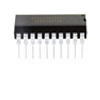
MC68HC908JK8CP Freescale Semiconductor, MC68HC908JK8CP Datasheet - Page 96

MC68HC908JK8CP
Manufacturer Part Number
MC68HC908JK8CP
Description
Manufacturer
Freescale Semiconductor
Datasheet
1.MC68HC908JK8CP.pdf
(212 pages)
Specifications of MC68HC908JK8CP
Cpu Family
HC08
Device Core Size
8b
Frequency (max)
8MHz
Interface Type
SCI
Program Memory Type
Flash
Program Memory Size
8KB
Total Internal Ram Size
256Byte
# I/os (max)
15
Number Of Timers - General Purpose
4
Operating Supply Voltage (typ)
3.3/5V
Operating Supply Voltage (max)
5.5V
Operating Supply Voltage (min)
2.7V
On-chip Adc
13-chx8-bit
Instruction Set Architecture
CISC
Operating Temp Range
-40C to 85C
Operating Temperature Classification
Industrial
Mounting
Through Hole
Pin Count
20
Package Type
PDIP
Lead Free Status / Rohs Status
Not Compliant
Available stocks
Company
Part Number
Manufacturer
Quantity
Price
Company:
Part Number:
MC68HC908JK8CP
Manufacturer:
ALTERA
Quantity:
13
Company:
Part Number:
MC68HC908JK8CPE
Manufacturer:
FREESCALE
Quantity:
928
Part Number:
MC68HC908JK8CPE
Manufacturer:
FREESCALE
Quantity:
20 000
- Current page: 96 of 212
- Download datasheet (2Mb)
Monitor ROM (MON)
The control and data bytes are described below.
7.5.1 PRGRNGE
PRGRNGE is used to program a range of FLASH locations with data loaded into the data array.
The start location of the FLASH to be programmed is specified by the address ADDRH:ADDRL and the
number of bytes from this location is specified by DATASIZE. The maximum number of bytes that can be
programmed in one routine call is 128 bytes (max. DATASIZE is 128).
ADDRH:ADDRL do not need to be at a page boundary, the routine handles any boundary misalignment
during programming. A check to see that all bytes in the specified range are erased is not performed by
this routine prior programming. Nor does this routine do a verification after programming, so there is no
return confirmation that programming was successful. User must assure that the range specified is first
erased.
The coding example below is to program 32 bytes of data starting at FLASH location $EF00, with a bus
speed of 4.9152 MHz. The coding assumes the data block is already loaded in RAM, with the address
pointer, FILE_PTR, pointing to the first byte of the data block.
96
•
•
•
•
Bus speed — This one byte indicates the operating bus speed of the MCU. The value of this byte
should be equal to 4 times the bus speed, and should not be set to less than 4 (i.e. minimum bus
speed is 1MHz).
Data size — This one byte indicates the number of bytes in the data array that are to be
manipulated. The maximum data array size is 128. Routines EE_WRITE and EE_READ are
restricted to manipulate a data array between 2 to 15 bytes. Whereas routines ERARNGE and
MON_ERARNGE do not manipulate a data array, thus, this data size byte has no meaning.
Start address — These two bytes, high byte followed by low byte, indicate the start address of the
FLASH memory to be manipulated.
Data array — This data array contains data that are to be manipulated. Data in this array are
programmed to FLASH memory by the programming routines: PRGRNGE, MON_PRGRNGE,
EE_WRITE. For the read routines: LDRNGE, MON_LDRNGE, and EE_READ, data is read from
FLASH and stored in this array.
Routine Name
Routine Description
Calling Address
Stack Used
Data Block Format
MC68HC908JL8/JK8 • MC68HC08JL8/JK8 • MC68HC908KL8 Data Sheet, Rev. 3.1
Table 7-11. PRGRNGE Routine
PRGRNGE
Program a range of locations
$FC06
15 bytes
Bus speed (BUS_SPD)
Data size (DATASIZE)
Start address high (ADDRH)
Start address (ADDRL)
Data 1 (DATA1)
Data N (DATAN)
:
Freescale Semiconductor
Related parts for MC68HC908JK8CP
Image
Part Number
Description
Manufacturer
Datasheet
Request
R
Part Number:
Description:
Manufacturer:
Freescale Semiconductor, Inc
Datasheet:
Part Number:
Description:
Manufacturer:
Freescale Semiconductor, Inc
Datasheet:
Part Number:
Description:
Manufacturer:
Freescale Semiconductor, Inc
Datasheet:
Part Number:
Description:
Manufacturer:
Freescale Semiconductor, Inc
Datasheet:
Part Number:
Description:
Manufacturer:
Freescale Semiconductor, Inc
Datasheet:
Part Number:
Description:
Manufacturer:
Freescale Semiconductor, Inc
Datasheet:
Part Number:
Description:
Manufacturer:
Freescale Semiconductor, Inc
Datasheet:
Part Number:
Description:
Manufacturer:
Freescale Semiconductor, Inc
Datasheet:
Part Number:
Description:
Manufacturer:
Freescale Semiconductor, Inc
Datasheet:
Part Number:
Description:
Manufacturer:
Freescale Semiconductor, Inc
Datasheet:
Part Number:
Description:
Manufacturer:
Freescale Semiconductor, Inc
Datasheet:
Part Number:
Description:
Manufacturer:
Freescale Semiconductor, Inc
Datasheet:
Part Number:
Description:
Manufacturer:
Freescale Semiconductor, Inc
Datasheet:
Part Number:
Description:
Manufacturer:
Freescale Semiconductor, Inc
Datasheet:
Part Number:
Description:
Manufacturer:
Freescale Semiconductor, Inc
Datasheet:


