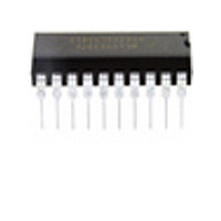
MC68HC908JK8CP Freescale Semiconductor, MC68HC908JK8CP Datasheet - Page 125

MC68HC908JK8CP
Manufacturer Part Number
MC68HC908JK8CP
Description
Manufacturer
Freescale Semiconductor
Datasheet
1.MC68HC908JK8CP.pdf
(212 pages)
Specifications of MC68HC908JK8CP
Cpu Family
HC08
Device Core Size
8b
Frequency (max)
8MHz
Interface Type
SCI
Program Memory Type
Flash
Program Memory Size
8KB
Total Internal Ram Size
256Byte
# I/os (max)
15
Number Of Timers - General Purpose
4
Operating Supply Voltage (typ)
3.3/5V
Operating Supply Voltage (max)
5.5V
Operating Supply Voltage (min)
2.7V
On-chip Adc
13-chx8-bit
Instruction Set Architecture
CISC
Operating Temp Range
-40C to 85C
Operating Temperature Classification
Industrial
Mounting
Through Hole
Pin Count
20
Package Type
PDIP
Lead Free Status / Rohs Status
Not Compliant
Available stocks
Company
Part Number
Manufacturer
Quantity
Price
Company:
Part Number:
MC68HC908JK8CP
Manufacturer:
ALTERA
Quantity:
13
Company:
Part Number:
MC68HC908JK8CPE
Manufacturer:
FREESCALE
Quantity:
928
Part Number:
MC68HC908JK8CPE
Manufacturer:
FREESCALE
Quantity:
20 000
At the start of a transmission, transmitter control logic automatically loads the transmit shift register with
a preamble of logic 1s. After the preamble shifts out, control logic transfers the SCDR data into the
transmit shift register. A logic 0 start bit automatically goes into the least significant bit position of the
transmit shift register. A logic 1 stop bit goes into the most significant bit position.
The SCI transmitter empty bit, SCTE, in SCS1 becomes set when the SCDR transfers a byte to the
transmit shift register. The SCTE bit indicates that the SCDR can accept new data from the internal data
bus. If the SCI transmit interrupt enable bit, SCTIE, in SCC2 is also set, the SCTE bit generates a
transmitter CPU interrupt request.
When the transmit shift register is not transmitting a character, the TxD pin goes to the idle condition, logic
1. If at any time software clears the ENSCI bit in SCI control register 1 (SCC1), the transmitter and
receiver relinquish control of the port pin.
9.4.2.3 Break Characters
Writing a logic 1 to the send break bit, SBK, in SCC2 loads the transmit shift register with a break
character. A break character contains all logic 0s and has no start, stop, or parity bit. Break character
length depends on the M bit in SCC1. As long as SBK is at logic 1, transmitter logic continuously loads
break characters into the transmit shift register. After software clears the SBK bit, the shift register finishes
transmitting the last break character and then transmits at least one logic 1. The automatic logic 1 at the
end of a break character guarantees the recognition of the start bit of the next character.
The SCI recognizes a break character when a start bit is followed by eight or nine logic 0 data bits and a
logic 0 where the stop bit should be.
Receiving a break character has these effects on SCI registers:
9.4.2.4 Idle Characters
An idle character contains all logic 1s and has no start, stop, or parity bit. Idle character length depends
on the M bit in SCC1. The preamble is a synchronizing idle character that begins every transmission.
If the TE bit is cleared during a transmission, the TxD pin becomes idle after completion of the
transmission in progress. Clearing and then setting the TE bit during a transmission queues an idle
character to be sent after the character currently being transmitted.
Freescale Semiconductor
1. Enable the SCI by writing a logic 1 to the enable SCI bit (ENSCI) in SCI control register 1 (SCC1).
2. Enable the transmitter by writing a logic 1 to the transmitter enable bit (TE) in SCI control register
3. Clear the SCI transmitter empty bit by first reading SCI status register 1 (SCS1) and then writing
4. Repeat step 3 for each subsequent transmission.
•
•
•
•
•
•
2 (SCC2).
to the SCDR.
Sets the framing error bit (FE) in SCS1
Sets the SCI receiver full bit (SCRF) in SCS1
Clears the SCI data register (SCDR)
Clears the R8 bit in SCC3
Sets the break flag bit (BKF) in SCS2
May set the overrun (OR), noise flag (NF), parity error (PE), or reception in progress flag (RPF) bits
MC68HC908JL8/JK8 • MC68HC08JL8/JK8 • MC68HC908KL8 Data Sheet, Rev. 3.1
Functional Description
125


