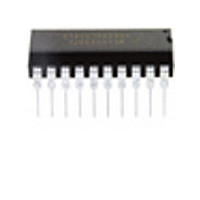
MC68HC908JK8CP Freescale Semiconductor, MC68HC908JK8CP Datasheet - Page 160

MC68HC908JK8CP
Manufacturer Part Number
MC68HC908JK8CP
Description
Manufacturer
Freescale Semiconductor
Datasheet
1.MC68HC908JK8CP.pdf
(212 pages)
Specifications of MC68HC908JK8CP
Cpu Family
HC08
Device Core Size
8b
Frequency (max)
8MHz
Interface Type
SCI
Program Memory Type
Flash
Program Memory Size
8KB
Total Internal Ram Size
256Byte
# I/os (max)
15
Number Of Timers - General Purpose
4
Operating Supply Voltage (typ)
3.3/5V
Operating Supply Voltage (max)
5.5V
Operating Supply Voltage (min)
2.7V
On-chip Adc
13-chx8-bit
Instruction Set Architecture
CISC
Operating Temp Range
-40C to 85C
Operating Temperature Classification
Industrial
Mounting
Through Hole
Pin Count
20
Package Type
PDIP
Lead Free Status / Rohs Status
Not Compliant
Available stocks
Company
Part Number
Manufacturer
Quantity
Price
Company:
Part Number:
MC68HC908JK8CP
Manufacturer:
ALTERA
Quantity:
13
Company:
Part Number:
MC68HC908JK8CPE
Manufacturer:
FREESCALE
Quantity:
928
Part Number:
MC68HC908JK8CPE
Manufacturer:
FREESCALE
Quantity:
20 000
- Current page: 160 of 212
- Download datasheet (2Mb)
Input/Output (I/O) Ports
11.4.3 Port D Control Register (PDCR)
The port D control register enables/disables the pull-up resistor and slow-edge high current capability of
pins PTD6 and PTD7.
SLOWDx — Slow Edge Enable
PTDPUx — Port D Pull-up Enable Bits
11.5 Port E
Port E is a 2-bit special function port that shares its pins with the timer 2 interface module (see
11.5.1 Port E Data Register (PTE)
The port E data register contains a data latch for each of the two port E pins.
PTE[1:0] — Port E Data Bits
160
The SLOWD6 and SLOWD7 bits enable the slow-edge, open-drain, high current output (25mA sink)
of port pins PTD6 and PTD7 respectively. DDRDx bit is not affected by SLOWDx.
The PTDPU6 and PTDPU7 bits enable the pull-up device on PTD6 and PTD7 respectively, regardless
the status of DDRDx bit.
These read/write bits are software programmable. Data direction of each port E pin is under the control
of the corresponding bit in data direction register E. Reset has no effect on port D data.
1 = Slow edge enabled; pin is open-drain output
0 = Slow edge disabled; pin is push-pull (standard I/O)
1 = Enable pull-up device
0 = Disable pull-up device
Alternative Functions:
Address:
Reset:
Read:
Write:
MC68HC908JL8/JK8 • MC68HC08JL8/JK8 • MC68HC908KL8 Data Sheet, Rev. 3.1
Address:
Reset:
Read:
Write:
$000A
Bit 7
0
0
PTE0–PTE1 are available on 32-pin packages only.
Figure 11-13. Port D Control Register (PDCR)
$0008
Bit 7
Figure 11-14. Port E Data Register (PTE)
6
0
0
6
5
0
0
5
NOTE
4
0
0
Unaffected by reset
4
SLOWD7
3
0
3
SLOWD6
2
0
2
PTDPU7
1
0
T2CH1
PTE1
1
Freescale Semiconductor
PTDPU6
Bit 0
0
T2CH0
PTE0
Bit 0
Chapter
8).
Related parts for MC68HC908JK8CP
Image
Part Number
Description
Manufacturer
Datasheet
Request
R
Part Number:
Description:
Manufacturer:
Freescale Semiconductor, Inc
Datasheet:
Part Number:
Description:
Manufacturer:
Freescale Semiconductor, Inc
Datasheet:
Part Number:
Description:
Manufacturer:
Freescale Semiconductor, Inc
Datasheet:
Part Number:
Description:
Manufacturer:
Freescale Semiconductor, Inc
Datasheet:
Part Number:
Description:
Manufacturer:
Freescale Semiconductor, Inc
Datasheet:
Part Number:
Description:
Manufacturer:
Freescale Semiconductor, Inc
Datasheet:
Part Number:
Description:
Manufacturer:
Freescale Semiconductor, Inc
Datasheet:
Part Number:
Description:
Manufacturer:
Freescale Semiconductor, Inc
Datasheet:
Part Number:
Description:
Manufacturer:
Freescale Semiconductor, Inc
Datasheet:
Part Number:
Description:
Manufacturer:
Freescale Semiconductor, Inc
Datasheet:
Part Number:
Description:
Manufacturer:
Freescale Semiconductor, Inc
Datasheet:
Part Number:
Description:
Manufacturer:
Freescale Semiconductor, Inc
Datasheet:
Part Number:
Description:
Manufacturer:
Freescale Semiconductor, Inc
Datasheet:
Part Number:
Description:
Manufacturer:
Freescale Semiconductor, Inc
Datasheet:
Part Number:
Description:
Manufacturer:
Freescale Semiconductor, Inc
Datasheet:


