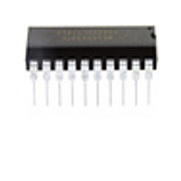
MC68HC908JK8CP Freescale Semiconductor, MC68HC908JK8CP Datasheet - Page 135

MC68HC908JK8CP
Manufacturer Part Number
MC68HC908JK8CP
Description
Manufacturer
Freescale Semiconductor
Datasheet
1.MC68HC908JK8CP.pdf
(212 pages)
Specifications of MC68HC908JK8CP
Cpu Family
HC08
Device Core Size
8b
Frequency (max)
8MHz
Interface Type
SCI
Program Memory Type
Flash
Program Memory Size
8KB
Total Internal Ram Size
256Byte
# I/os (max)
15
Number Of Timers - General Purpose
4
Operating Supply Voltage (typ)
3.3/5V
Operating Supply Voltage (max)
5.5V
Operating Supply Voltage (min)
2.7V
On-chip Adc
13-chx8-bit
Instruction Set Architecture
CISC
Operating Temp Range
-40C to 85C
Operating Temperature Classification
Industrial
Mounting
Through Hole
Pin Count
20
Package Type
PDIP
Lead Free Status / Rohs Status
Not Compliant
Available stocks
Company
Part Number
Manufacturer
Quantity
Price
Company:
Part Number:
MC68HC908JK8CP
Manufacturer:
ALTERA
Quantity:
13
Company:
Part Number:
MC68HC908JK8CPE
Manufacturer:
FREESCALE
Quantity:
928
Part Number:
MC68HC908JK8CPE
Manufacturer:
FREESCALE
Quantity:
20 000
- Current page: 135 of 212
- Download datasheet (2Mb)
M — Mode (Character Length) Bit
WAKE — Wakeup Condition Bit
ILTY — Idle Line Type Bit
PEN — Parity Enable Bit
PTY — Parity Bit
Freescale Semiconductor
This read/write bit determines whether SCI characters are eight or nine bits long. (See
ninth bit can serve as an extra stop bit, as a receiver wakeup signal, or as a parity bit. Reset clears the
M bit.
This read/write bit determines which condition wakes up the SCI: a logic 1 (address mark) in the most
significant bit position of a received character or an idle condition on the RxD pin. Reset clears the
WAKE bit.
This read/write bit determines when the SCI starts counting logic 1s as idle character bits. The counting
begins either after the start bit or after the stop bit. If the count begins after the start bit, then a string
of logic 1s preceding the stop bit may cause false recognition of an idle character. Beginning the count
after the stop bit avoids false idle character recognition, but requires properly synchronized
transmissions. Reset clears the ILTY bit.
This read/write bit enables the SCI parity function. (See
inserts a parity bit in the most significant bit position. (See
This read/write bit determines whether the SCI generates and checks for odd parity or even parity.
(See
1 = 9-bit SCI characters
0 = 8-bit SCI characters
1 = Address mark wakeup
0 = Idle line wakeup
1 = Idle character bit count begins after stop bit
0 = Idle character bit count begins after start bit
1 = Parity function enabled
0 = Parity function disabled
1 = Odd parity
0 = Even parity
Table
9-5.) Reset clears the PTY bit.
Changing the PTY bit in the middle of a transmission or reception can
generate a parity error.
M
0
1
0
0
1
1
MC68HC908JL8/JK8 • MC68HC08JL8/JK8 • MC68HC908KL8 Data Sheet, Rev. 3.1
Control Bits
PEN and PTY
0X
0X
10
11
10
11
Table 9-5. Character Format Selection
Start
Bits
1
1
1
1
1
1
Data
Bits
NOTE
8
9
7
7
8
8
Character Format
Parity
None
None
Even
Even
Table
Odd
Odd
Figure
9-5.) When enabled, the parity function
9-3.) Reset clears the PEN bit.
Stop
Bits
1
1
1
1
1
1
Character
Length
10 bits
11 bits
10 bits
10 bits
11 bits
11 bits
Table
I/O Registers
9-5.) The
135
Related parts for MC68HC908JK8CP
Image
Part Number
Description
Manufacturer
Datasheet
Request
R
Part Number:
Description:
Manufacturer:
Freescale Semiconductor, Inc
Datasheet:
Part Number:
Description:
Manufacturer:
Freescale Semiconductor, Inc
Datasheet:
Part Number:
Description:
Manufacturer:
Freescale Semiconductor, Inc
Datasheet:
Part Number:
Description:
Manufacturer:
Freescale Semiconductor, Inc
Datasheet:
Part Number:
Description:
Manufacturer:
Freescale Semiconductor, Inc
Datasheet:
Part Number:
Description:
Manufacturer:
Freescale Semiconductor, Inc
Datasheet:
Part Number:
Description:
Manufacturer:
Freescale Semiconductor, Inc
Datasheet:
Part Number:
Description:
Manufacturer:
Freescale Semiconductor, Inc
Datasheet:
Part Number:
Description:
Manufacturer:
Freescale Semiconductor, Inc
Datasheet:
Part Number:
Description:
Manufacturer:
Freescale Semiconductor, Inc
Datasheet:
Part Number:
Description:
Manufacturer:
Freescale Semiconductor, Inc
Datasheet:
Part Number:
Description:
Manufacturer:
Freescale Semiconductor, Inc
Datasheet:
Part Number:
Description:
Manufacturer:
Freescale Semiconductor, Inc
Datasheet:
Part Number:
Description:
Manufacturer:
Freescale Semiconductor, Inc
Datasheet:
Part Number:
Description:
Manufacturer:
Freescale Semiconductor, Inc
Datasheet:


