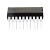
MC68HC908JK8CP Freescale Semiconductor, MC68HC908JK8CP Datasheet - Page 147

MC68HC908JK8CP
Manufacturer Part Number
MC68HC908JK8CP
Description
Manufacturer
Freescale Semiconductor
Datasheet
1.MC68HC908JK8CP.pdf
(212 pages)
Specifications of MC68HC908JK8CP
Cpu Family
HC08
Device Core Size
8b
Frequency (max)
8MHz
Interface Type
SCI
Program Memory Type
Flash
Program Memory Size
8KB
Total Internal Ram Size
256Byte
# I/os (max)
15
Number Of Timers - General Purpose
4
Operating Supply Voltage (typ)
3.3/5V
Operating Supply Voltage (max)
5.5V
Operating Supply Voltage (min)
2.7V
On-chip Adc
13-chx8-bit
Instruction Set Architecture
CISC
Operating Temp Range
-40C to 85C
Operating Temperature Classification
Industrial
Mounting
Through Hole
Pin Count
20
Package Type
PDIP
Lead Free Status / Rohs Status
Not Compliant
Available stocks
Company
Part Number
Manufacturer
Quantity
Price
Company:
Part Number:
MC68HC908JK8CP
Manufacturer:
ALTERA
Quantity:
13
Company:
Part Number:
MC68HC908JK8CPE
Manufacturer:
FREESCALE
Quantity:
928
Part Number:
MC68HC908JK8CPE
Manufacturer:
FREESCALE
Quantity:
20 000
- Current page: 147 of 212
- Download datasheet (2Mb)
Interrupts
10.3.2 Voltage Conversion
When the input voltage to the ADC equals V
, the ADC converts the signal to $FF (full scale). If the input
DD
voltage equals V
, the ADC converts it to $00. Input voltages between V
and V
are a straight-line
SS
DD
SS
linear conversion. All other input voltages will result in $FF if greater than V
and $00 if less than V
.
DD
SS
NOTE
Input voltage should not exceed the analog supply voltages.
10.3.3 Conversion Time
Fourteen ADC internal clocks are required to perform one conversion. The ADC starts a conversion on
the first rising edge of the ADC internal clock immediately following a write to the ADSCR. If the ADC
internal clock is selected to run at 1MHz, then one conversion will take 14µs to complete. With a 1MHz
ADC internal clock the maximum sample rate is 71.43kHz.
14 ADC Clock Cycles
Conversion Time =
ADC Clock Frequency
Number of Bus Cycles = Conversion Time × Bus Frequency
10.3.4 Continuous Conversion
In the continuous conversion mode, the ADC continuously converts the selected channel filling the ADC
data register with new data after each conversion. Data from the previous conversion will be overwritten
whether that data has been read or not. Conversions will continue until the ADCO bit is cleared. The
COCO bit (ADC status and control register, $003C) is set after each conversion and can be cleared by
writing the ADC status and control register or reading of the ADC data register.
10.3.5 Accuracy and Precision
The conversion process is monotonic and has no missing codes.
10.4 Interrupts
When the AIEN bit is set, the ADC module is capable of generating a CPU interrupt after each ADC
conversion. A CPU interrupt is generated if the COCO bit is at logic 0. The COCO bit is not used as a
conversion complete flag when interrupts are enabled.
10.5 Low-Power Modes
The following subsections describe the ADC in low-power modes.
10.5.1 Wait Mode
The ADC continues normal operation during wait mode. Any enabled CPU interrupt request from the ADC
can bring the MCU out of wait mode. If the ADC is not required to bring the MCU out of wait mode, power
down the ADC by setting the ADCH[4:0] bits in the ADC status and control register to logic 1’s before
executing the WAIT instruction.
MC68HC908JL8/JK8 • MC68HC08JL8/JK8 • MC68HC908KL8 Data Sheet, Rev. 3.1
Freescale Semiconductor
147
Related parts for MC68HC908JK8CP
Image
Part Number
Description
Manufacturer
Datasheet
Request
R
Part Number:
Description:
Manufacturer:
Freescale Semiconductor, Inc
Datasheet:
Part Number:
Description:
Manufacturer:
Freescale Semiconductor, Inc
Datasheet:
Part Number:
Description:
Manufacturer:
Freescale Semiconductor, Inc
Datasheet:
Part Number:
Description:
Manufacturer:
Freescale Semiconductor, Inc
Datasheet:
Part Number:
Description:
Manufacturer:
Freescale Semiconductor, Inc
Datasheet:
Part Number:
Description:
Manufacturer:
Freescale Semiconductor, Inc
Datasheet:
Part Number:
Description:
Manufacturer:
Freescale Semiconductor, Inc
Datasheet:
Part Number:
Description:
Manufacturer:
Freescale Semiconductor, Inc
Datasheet:
Part Number:
Description:
Manufacturer:
Freescale Semiconductor, Inc
Datasheet:
Part Number:
Description:
Manufacturer:
Freescale Semiconductor, Inc
Datasheet:
Part Number:
Description:
Manufacturer:
Freescale Semiconductor, Inc
Datasheet:
Part Number:
Description:
Manufacturer:
Freescale Semiconductor, Inc
Datasheet:
Part Number:
Description:
Manufacturer:
Freescale Semiconductor, Inc
Datasheet:
Part Number:
Description:
Manufacturer:
Freescale Semiconductor, Inc
Datasheet:
Part Number:
Description:
Manufacturer:
Freescale Semiconductor, Inc
Datasheet:


