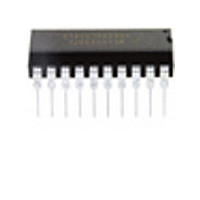
MC68HC908JK8CP Freescale Semiconductor, MC68HC908JK8CP Datasheet - Page 194

MC68HC908JK8CP
Manufacturer Part Number
MC68HC908JK8CP
Description
Manufacturer
Freescale Semiconductor
Datasheet
1.MC68HC908JK8CP.pdf
(212 pages)
Specifications of MC68HC908JK8CP
Cpu Family
HC08
Device Core Size
8b
Frequency (max)
8MHz
Interface Type
SCI
Program Memory Type
Flash
Program Memory Size
8KB
Total Internal Ram Size
256Byte
# I/os (max)
15
Number Of Timers - General Purpose
4
Operating Supply Voltage (typ)
3.3/5V
Operating Supply Voltage (max)
5.5V
Operating Supply Voltage (min)
2.7V
On-chip Adc
13-chx8-bit
Instruction Set Architecture
CISC
Operating Temp Range
-40C to 85C
Operating Temperature Classification
Industrial
Mounting
Through Hole
Pin Count
20
Package Type
PDIP
Lead Free Status / Rohs Status
Not Compliant
Available stocks
Company
Part Number
Manufacturer
Quantity
Price
Company:
Part Number:
MC68HC908JK8CP
Manufacturer:
ALTERA
Quantity:
13
Company:
Part Number:
MC68HC908JK8CPE
Manufacturer:
FREESCALE
Quantity:
928
Part Number:
MC68HC908JK8CPE
Manufacturer:
FREESCALE
Quantity:
20 000
- Current page: 194 of 212
- Download datasheet (2Mb)
Electrical Specifications
17.14 Memory Characteristics
194
RAM
FLASH program bus clock frequency
FLASH
FLASH
FLASH
FLASH PGM
FLASH
FLASH
FLASH
FLASH
FLASH
FLASH
FLASH
FLASH
FLASH
1. f
2. If the page erase time is longer than t
3. If the mass erase time is longer than t
4. t
5. t
6. The minimum row endurance value specifies each row of the FLASH memory is guaranteed to work for at least this many
7. The minimum row endurance value specifies each row of the FLASH memory is guaranteed to work for at least this many
8. The FLASH is guaranteed to retain data over the entire operating temperature range for at least the minimum time speci-
memory.
memory.
HVEN to logic 0.
t
erase / program cycles.
erase / program cycles.
fied.
rcv
read
HV
HV
data retention voltage
is defined as the time it needs before the FLASH can be read after turning off the high voltage charge pump, by clearing
is defined as the cumulative high voltage programming time to the same row before next erase.
must satisfy this condition: t
is defined as the frequency range for which the FLASH memory can be read.
read bus clock frequency
page erase time
mass erase time
high-voltage hold time
high-voltage hold time (mass erase)
program hold time
program time
return to read time
cumulative program hv period
row erase enduran
row program end
data retention t
/
ERASE
MC68HC908JL8/JK8 • MC68HC08JL8/JK8 • MC68HC908KL8 Data Sheet, Rev. 3.1
Characteristic
ime
to
urance
HVEN
ce
(8)
(6)
(7)
set up time
nvs
+ t
Table 17-12. Memory Characteristics
nvh
merase
erase
+ t
pgs
(Min), there is no erase-disturb, but it reduces the endurance of the FLASH
(Min), there is no erase-disturb, but it reduces the endurance of the FLASH
+ (t
prog
×
32) ≤ t
t
HV
Symbol
me
t
f
V
e
t
t
r
t
t
rcv
HV
rase
t
t
ead
t
prog
nvhl
RDR
—
nvh
pgs
—
—
—
rase
nvs
max.
(4)
(5)
(1)
(2)
(3)
32k
100
10k
10k
Min
1.3
10
30
10
—
1
4
4
5
5
1
Freescale Semiconductor
Max
8M
40
—
—
—
—
—
—
—
—
—
—
—
—
4
cycles
cycles
years
MHz
Unit
ms
ms
ms
Hz
µs
µs
µs
µs
µs
µs
V
Related parts for MC68HC908JK8CP
Image
Part Number
Description
Manufacturer
Datasheet
Request
R
Part Number:
Description:
Manufacturer:
Freescale Semiconductor, Inc
Datasheet:
Part Number:
Description:
Manufacturer:
Freescale Semiconductor, Inc
Datasheet:
Part Number:
Description:
Manufacturer:
Freescale Semiconductor, Inc
Datasheet:
Part Number:
Description:
Manufacturer:
Freescale Semiconductor, Inc
Datasheet:
Part Number:
Description:
Manufacturer:
Freescale Semiconductor, Inc
Datasheet:
Part Number:
Description:
Manufacturer:
Freescale Semiconductor, Inc
Datasheet:
Part Number:
Description:
Manufacturer:
Freescale Semiconductor, Inc
Datasheet:
Part Number:
Description:
Manufacturer:
Freescale Semiconductor, Inc
Datasheet:
Part Number:
Description:
Manufacturer:
Freescale Semiconductor, Inc
Datasheet:
Part Number:
Description:
Manufacturer:
Freescale Semiconductor, Inc
Datasheet:
Part Number:
Description:
Manufacturer:
Freescale Semiconductor, Inc
Datasheet:
Part Number:
Description:
Manufacturer:
Freescale Semiconductor, Inc
Datasheet:
Part Number:
Description:
Manufacturer:
Freescale Semiconductor, Inc
Datasheet:
Part Number:
Description:
Manufacturer:
Freescale Semiconductor, Inc
Datasheet:
Part Number:
Description:
Manufacturer:
Freescale Semiconductor, Inc
Datasheet:


