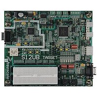
LFEBS12UB Freescale Semiconductor, LFEBS12UB Datasheet - Page 1208

LFEBS12UB
Manufacturer Part Number
LFEBS12UB
Description
KIT STUDENT LEARNING S12 DG128
Manufacturer
Freescale Semiconductor
Specifications of LFEBS12UB
Architecture
8/16-bit
Code Gen Tools Included
Code Warrior
Silicon Manufacturer
Freescale
Core Architecture
S12
Core Sub-architecture
S12
Silicon Core Number
MC9S12
Silicon Family Name
S12D
Kit Contents
HCS12 DG128 Learning Kit
Rohs Compliant
Yes
Lead Free Status / RoHS Status
Lead free / RoHS Compliant
- Current page: 1208 of 1328
- Download datasheet (9Mb)
Appendix A Electrical Characteristics
A.1.7
This section describes the operating conditions of the device. Unless otherwise noted those conditions
apply to all the following data.
1
2
3
4
1208
I/O, regulator and analog supply voltage
NVM logic supply voltage
Voltage difference V
Voltage difference V
Voltage difference V
Voltage difference V
Digital logic supply voltage
PLL supply voltage
Oscillator
(Full Swing Pierce)
Bus frequency
C Operating junction temperature range
V Operating junction temperature range
M Operating junction temperature range
The device contains an internal voltage regulator to generate the logic and PLL supply out of the I/O supply. .
This refers to the oscillator base frequency. Typical crystal & resonator tolerances are supported.
Please refer to
Please refer to
ambient temperature T
Operating ambient temperature range
Operating ambient temperature range
Operating ambient temperature range
2
(Loop Controlled Pierce)
Operating Conditions
3
Table A-25
Section A.1.8, “Power Dissipation and Thermal Characteristics”
Please refer to the temperature rating of the device (C, V, M) with regards to
the ambient temperature T
dissipation calculations refer to
Thermal
Using the internal voltage regulator, operation is guaranteed in a power
down until a low voltage reset assertion.
DDX
DDR
SSX
SS1
, V
to V
A
to V
to V
1
and device junction temperature T
1
SS2
Rating
Characteristics”.
SSA
for maximum bus frequency limits with frequency modulation enabled
DDA
DDX
, V
SS3
MC9S12XE-Family Reference Manual , Rev. 1.23
, V
SSPLL
4
2
2
Table A-4. Operating Conditions
to V
A
SSX
and the junction temperature T
Section A.1.8, “Power Dissipation and
NOTE
NOTE
J
.
Symbol
V
∆
∆
V
∆
V
∆
DDPLL
VDDR
V
VDDX
VSSX
f
f
DD35
VSS
T J
T A
T J
T A
T J
T A
DDF
osc
bus
DD
3.13
–0.1
–0.1
1.72
1.72
for more details about the relation between
Min
–40
–40
–40
–40
–40
–40
2.7
0.5
4
2
J
. For power
refer to
refer to
Typ
2.8
1.8
1.8
27
27
27
—
—
—
—
—
—
5
0
0
Table A-15
Table A-15
Freescale Semiconductor
Max
1.98
1.98
110
130
105
150
125
5.5
2.9
0.1
0.1
16
40
50
85
MHz
MHz
Unit
°C
°C
°C
V
V
V
V
V
V
Related parts for LFEBS12UB
Image
Part Number
Description
Manufacturer
Datasheet
Request
R
Part Number:
Description:
Manufacturer:
Freescale Semiconductor, Inc
Datasheet:
Part Number:
Description:
Manufacturer:
Freescale Semiconductor, Inc
Datasheet:
Part Number:
Description:
Manufacturer:
Freescale Semiconductor, Inc
Datasheet:
Part Number:
Description:
Manufacturer:
Freescale Semiconductor, Inc
Datasheet:
Part Number:
Description:
Manufacturer:
Freescale Semiconductor, Inc
Datasheet:
Part Number:
Description:
Manufacturer:
Freescale Semiconductor, Inc
Datasheet:
Part Number:
Description:
Manufacturer:
Freescale Semiconductor, Inc
Datasheet:
Part Number:
Description:
Manufacturer:
Freescale Semiconductor, Inc
Datasheet:
Part Number:
Description:
Manufacturer:
Freescale Semiconductor, Inc
Datasheet:
Part Number:
Description:
Manufacturer:
Freescale Semiconductor, Inc
Datasheet:
Part Number:
Description:
Manufacturer:
Freescale Semiconductor, Inc
Datasheet:
Part Number:
Description:
Manufacturer:
Freescale Semiconductor, Inc
Datasheet:
Part Number:
Description:
Manufacturer:
Freescale Semiconductor, Inc
Datasheet:
Part Number:
Description:
Manufacturer:
Freescale Semiconductor, Inc
Datasheet:
Part Number:
Description:
Manufacturer:
Freescale Semiconductor, Inc
Datasheet:


