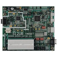
LFEBS12UB Freescale Semiconductor, LFEBS12UB Datasheet - Page 130

LFEBS12UB
Manufacturer Part Number
LFEBS12UB
Description
KIT STUDENT LEARNING S12 DG128
Manufacturer
Freescale Semiconductor
Specifications of LFEBS12UB
Architecture
8/16-bit
Code Gen Tools Included
Code Warrior
Silicon Manufacturer
Freescale
Core Architecture
S12
Core Sub-architecture
S12
Silicon Core Number
MC9S12
Silicon Family Name
S12D
Kit Contents
HCS12 DG128 Learning Kit
Rohs Compliant
Yes
Lead Free Status / RoHS Status
Lead free / RoHS Compliant
- Current page: 130 of 1328
- Download datasheet (9Mb)
1. Read: Anytime.
1. Read: Anytime.
Chapter 2 Port Integration Module (S12XEPIMV1)
2.3.30
2.3.31
130
Address 0x0249
Address 0x024A
Write:Never, writes to this register have no effect.
Write: Anytime.
Field
Field
PTIS
PTS
PTS
Reset
Reset
7-0
1
0
W
W
R
R
Port S general purpose input/output data—Data Register
Port S pin 3 is associated with the TXD signal of the SCI0 module.
When not used with the alternative function, this pin can be used as general purpose I/O.
If the associated data direction bit of this pin is set to 1, a read returns the value of the port register, otherwise the
buffered pin input state is read.
Port S general purpose input/output data—Data Register
Port S bits 2 is associated with the RXD signal of the SCI0 module.
When not used with the alternative function, this pin can be used as general purpose I/O.
If the associated data direction bit of this pin is set to 1, a read returns the value of the port register, otherwise the
buffered pin input state is read.
Port S input data—
This register always reads back the buffered state of the associated pins. This can also be used to detect overload
or short circuit conditions on output pins.
DDRS7
PTIS7
Port S Input Register (PTIS)
Port S Data Direction Register (DDRS)
u
0
7
7
= Unimplemented or Reserved
DDRS6
PTIS6
Table 2-26. PTS Register Field Descriptions (continued)
u
0
6
6
Figure 2-29. Port S Data Direction Register (DDRS)
Table 2-27. PTIS Register Field Descriptions
MC9S12XE-Family Reference Manual , Rev. 1.23
Figure 2-28. Port S Input Register (PTIS)
DDRS5
PTIS5
u
0
5
5
DDRS4
PTIS4
u
0
4
4
Description
Description
u = Unaffected by reset
DDRS3
PTIS3
3
u
3
0
DDRS2
PTIS2
u
0
2
2
Access: User read/write
Freescale Semiconductor
DDRS1
PTIS1
u
0
1
1
Access: User read
DDRS0
PTIS0
u
0
0
0
(1)
(1)
Related parts for LFEBS12UB
Image
Part Number
Description
Manufacturer
Datasheet
Request
R
Part Number:
Description:
Manufacturer:
Freescale Semiconductor, Inc
Datasheet:
Part Number:
Description:
Manufacturer:
Freescale Semiconductor, Inc
Datasheet:
Part Number:
Description:
Manufacturer:
Freescale Semiconductor, Inc
Datasheet:
Part Number:
Description:
Manufacturer:
Freescale Semiconductor, Inc
Datasheet:
Part Number:
Description:
Manufacturer:
Freescale Semiconductor, Inc
Datasheet:
Part Number:
Description:
Manufacturer:
Freescale Semiconductor, Inc
Datasheet:
Part Number:
Description:
Manufacturer:
Freescale Semiconductor, Inc
Datasheet:
Part Number:
Description:
Manufacturer:
Freescale Semiconductor, Inc
Datasheet:
Part Number:
Description:
Manufacturer:
Freescale Semiconductor, Inc
Datasheet:
Part Number:
Description:
Manufacturer:
Freescale Semiconductor, Inc
Datasheet:
Part Number:
Description:
Manufacturer:
Freescale Semiconductor, Inc
Datasheet:
Part Number:
Description:
Manufacturer:
Freescale Semiconductor, Inc
Datasheet:
Part Number:
Description:
Manufacturer:
Freescale Semiconductor, Inc
Datasheet:
Part Number:
Description:
Manufacturer:
Freescale Semiconductor, Inc
Datasheet:
Part Number:
Description:
Manufacturer:
Freescale Semiconductor, Inc
Datasheet:


