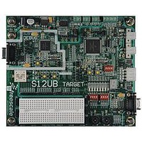
LFEBS12UB Freescale Semiconductor, LFEBS12UB Datasheet - Page 803

LFEBS12UB
Manufacturer Part Number
LFEBS12UB
Description
KIT STUDENT LEARNING S12 DG128
Manufacturer
Freescale Semiconductor
Specifications of LFEBS12UB
Architecture
8/16-bit
Code Gen Tools Included
Code Warrior
Silicon Manufacturer
Freescale
Core Architecture
S12
Core Sub-architecture
S12
Silicon Core Number
MC9S12
Silicon Family Name
S12D
Kit Contents
HCS12 DG128 Learning Kit
Rohs Compliant
Yes
Lead Free Status / RoHS Status
Lead free / RoHS Compliant
- Current page: 803 of 1328
- Download datasheet (9Mb)
Read: Anytime
Write: Anytime.
22.3.2.10 Timer Interrupt Enable Register (TIE)
Read: Anytime
Write: Anytime.
Freescale Semiconductor
Module Base + 0x000C
Because of an order from the United States International Trade Commission, BGA-packaged product lines and partnumbers
EDGnB
EDGnA
C7I:C0I
Reset
indicated here currently are not available from Freescale for import or sale in the United States prior to September 2010
Field
Field
7:0
7:0
W
R
Input Capture Edge Control — These eight pairs of control bits configure the input capture edge detector
circuits.
Input Capture/Output Compare “x” Interrupt Enable — The bits in TIE correspond bit-for-bit with the bits in
the TFLG1 status register. If cleared, the corresponding flag is disabled from causing a hardware interrupt. If set,
the corresponding flag is enabled to cause a interrupt.
C7I
0
7
C6I
0
6
EDGnB
Figure 22-18. Timer Interrupt Enable Register (TIE)
Table 22-12. Edge Detector Circuit Configuration
0
0
1
1
Table 22-11. TCTL3/TCTL4 Field Descriptions
MC9S12XE-Family Reference Manual Rev. 1.23
Table 22-13. TIE Field Descriptions
C5I
EDGnA
5
0
0
1
0
1
Capture on any edge (rising or falling)
C4I
0
4
Capture on falling edges only
Capture on rising edges only
Description
Description
Capture disabled
Configuration
Chapter 22 Timer Module (TIM16B8CV2) Block Description
C3I
0
3
C2I
2
0
C1I
0
1
C0I
0
0
803
Related parts for LFEBS12UB
Image
Part Number
Description
Manufacturer
Datasheet
Request
R
Part Number:
Description:
Manufacturer:
Freescale Semiconductor, Inc
Datasheet:
Part Number:
Description:
Manufacturer:
Freescale Semiconductor, Inc
Datasheet:
Part Number:
Description:
Manufacturer:
Freescale Semiconductor, Inc
Datasheet:
Part Number:
Description:
Manufacturer:
Freescale Semiconductor, Inc
Datasheet:
Part Number:
Description:
Manufacturer:
Freescale Semiconductor, Inc
Datasheet:
Part Number:
Description:
Manufacturer:
Freescale Semiconductor, Inc
Datasheet:
Part Number:
Description:
Manufacturer:
Freescale Semiconductor, Inc
Datasheet:
Part Number:
Description:
Manufacturer:
Freescale Semiconductor, Inc
Datasheet:
Part Number:
Description:
Manufacturer:
Freescale Semiconductor, Inc
Datasheet:
Part Number:
Description:
Manufacturer:
Freescale Semiconductor, Inc
Datasheet:
Part Number:
Description:
Manufacturer:
Freescale Semiconductor, Inc
Datasheet:
Part Number:
Description:
Manufacturer:
Freescale Semiconductor, Inc
Datasheet:
Part Number:
Description:
Manufacturer:
Freescale Semiconductor, Inc
Datasheet:
Part Number:
Description:
Manufacturer:
Freescale Semiconductor, Inc
Datasheet:
Part Number:
Description:
Manufacturer:
Freescale Semiconductor, Inc
Datasheet:


