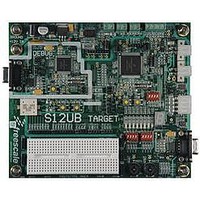
LFEBS12UB Freescale Semiconductor, LFEBS12UB Datasheet - Page 62

LFEBS12UB
Manufacturer Part Number
LFEBS12UB
Description
KIT STUDENT LEARNING S12 DG128
Manufacturer
Freescale Semiconductor
Specifications of LFEBS12UB
Architecture
8/16-bit
Code Gen Tools Included
Code Warrior
Silicon Manufacturer
Freescale
Core Architecture
S12
Core Sub-architecture
S12
Silicon Core Number
MC9S12
Silicon Family Name
S12D
Kit Contents
HCS12 DG128 Learning Kit
Rohs Compliant
Yes
Lead Free Status / RoHS Status
Lead free / RoHS Compliant
- Current page: 62 of 1328
- Download datasheet (9Mb)
Chapter 1 Device Overview MC9S12XE-Family
1.2.3
1.2.3.1
EXTAL and XTAL are the crystal driver and external clock pins. On reset all the device clocks are derived
from the EXTAL input frequency. XTAL is the oscillator output.
1.2.3.2
The RESET pin is an active low bidirectional control signal. It acts as an input to initialize the MCU to a
known start-up state. As an output it is driven low to indicate when any internal MCU reset source triggers.
The RESET pin has an internal pull-up device.
1.2.3.3
This input only pin is reserved for test. This pin has a pull-down device.
1.2.3.4
The BKGD/MODC pin is used as a pseudo-open-drain pin for the background debug communication. It
is used as a MCU operating mode select pin during reset. The state of this pin is latched to the MODC bit
at the rising edge of RESET. The BKGD pin has a pull-up device.
1.2.3.5
PAD[15:0] are general-purpose input or output pins and analog inputs AN[15:0] of the analog-to-digital
converter ATD0.
1.2.3.6
PAD[31:16] are general-purpose input or output pins and analog inputs AN[31:16] of the analog-to-digital
converter ATD1.
62
Because of an order from the United States International Trade Commission, BGA-packaged product lines and partnumbers
indicated here currently are not available from Freescale for import or sale in the United States prior to September 2010
Detailed Signal Descriptions
EXTAL, XTAL — Oscillator Pins
RESET — External Reset Pin
TEST — Test Pin
BKGD / MODC — Background Debug and Mode Pin
PAD[15:0] / AN[15:0] — Port AD Input Pins of ATD0
PAD[31:16] / AN[31:16] — Port AD Input Pins of ATD1
The pin list of the largest package version of each MC9S12XE-Family
derivative gives the complete of interface signals that also exist on smaller
package options, although some of them are not bonded out. For devices
assembled in smaller packages all non-bonded out pins should be
configured as outputs after reset in order to avoid current drawn from
floating inputs. Refer to
drawn to Port R, which does not have enabled pull-up/pull-down devices
coming out of reset.
The TEST pin must be tied to V
MC9S12XE-Family Reference Manual , Rev. 1.23
Table 1-10
SS
NOTE
NOTE
in all applications.
for affected pins. Particular attention is
Freescale Semiconductor
Related parts for LFEBS12UB
Image
Part Number
Description
Manufacturer
Datasheet
Request
R
Part Number:
Description:
Manufacturer:
Freescale Semiconductor, Inc
Datasheet:
Part Number:
Description:
Manufacturer:
Freescale Semiconductor, Inc
Datasheet:
Part Number:
Description:
Manufacturer:
Freescale Semiconductor, Inc
Datasheet:
Part Number:
Description:
Manufacturer:
Freescale Semiconductor, Inc
Datasheet:
Part Number:
Description:
Manufacturer:
Freescale Semiconductor, Inc
Datasheet:
Part Number:
Description:
Manufacturer:
Freescale Semiconductor, Inc
Datasheet:
Part Number:
Description:
Manufacturer:
Freescale Semiconductor, Inc
Datasheet:
Part Number:
Description:
Manufacturer:
Freescale Semiconductor, Inc
Datasheet:
Part Number:
Description:
Manufacturer:
Freescale Semiconductor, Inc
Datasheet:
Part Number:
Description:
Manufacturer:
Freescale Semiconductor, Inc
Datasheet:
Part Number:
Description:
Manufacturer:
Freescale Semiconductor, Inc
Datasheet:
Part Number:
Description:
Manufacturer:
Freescale Semiconductor, Inc
Datasheet:
Part Number:
Description:
Manufacturer:
Freescale Semiconductor, Inc
Datasheet:
Part Number:
Description:
Manufacturer:
Freescale Semiconductor, Inc
Datasheet:
Part Number:
Description:
Manufacturer:
Freescale Semiconductor, Inc
Datasheet:


