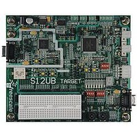
LFEBS12UB Freescale Semiconductor, LFEBS12UB Datasheet - Page 828

LFEBS12UB
Manufacturer Part Number
LFEBS12UB
Description
KIT STUDENT LEARNING S12 DG128
Manufacturer
Freescale Semiconductor
Specifications of LFEBS12UB
Architecture
8/16-bit
Code Gen Tools Included
Code Warrior
Silicon Manufacturer
Freescale
Core Architecture
S12
Core Sub-architecture
S12
Silicon Core Number
MC9S12
Silicon Family Name
S12D
Kit Contents
HCS12 DG128 Learning Kit
Rohs Compliant
Yes
Lead Free Status / RoHS Status
Lead free / RoHS Compliant
- Current page: 828 of 1328
- Download datasheet (9Mb)
Chapter 23 Voltage Regulator (S12VREGL3V3V1)
23.4
23.4.1
Module VREG_3V3 is a voltage regulator, as depicted in
are the regulator core (REG), a low-voltage detect module (LVD), a control block (CTRL), a power-on
reset module (POR), and a low-voltage reset module (LVR)and a high temperature sensor (HTD).
23.4.2
Respectively its regulator core has three parallel, independent regulation loops (REG1,REG2 and REG3).
REG1 and REG3 differ only in the amount of current that can be delivered.
The regulators are linear regulator with a bandgap reference when operated in Full Performance Mode.
They act as a voltage clamp in Reduced Power Mode. All load currents flow from input VDDR to VSS or
VSSPLL. The reference circuits are supplied by VDDA and VSSA.
23.4.2.1
In Full Performance Mode, the output voltage is compared with a reference voltage by an operational
amplifier. The amplified input voltage difference drives the gate of an output transistor.
23.4.2.2
In Reduced Power Mode, the gate of the output transistor is connected directly to a reference voltage to
reduce power consumption. Mode switching from reduced power to full performance requires a transition
time of t
23.4.3
Subblock LVD is responsible for generating the low-voltage interrupt (LVI). LVD monitors the input
voltage (V
status flag LVDS changes its value. The LVD is available in FPM and is inactive in Reduced Power Mode
or Shutdown Mode.
828
Because of an order from the United States International Trade Commission, BGA-packaged product lines and partnumbers
indicated here currently are not available from Freescale for import or sale in the United States prior to September 2010
vup
Functional Description
DDA
, if the voltage regulator is enabled.
General
Regulator Core (REG)
Low-Voltage Detect (LVD)
Full Performance Mode
Reduced Power Mode
–V
SSA
) and continuously updates the status flag LVDS. Interrupt flag LVIF is set whenever
HTTR[2]
HTTR[1]
HTTR[0]
Bit
MC9S12XE-Family Reference Manual , Rev. 1.23
Table 23-11. Trimming Effect (continued)
Increases V
Increases V
Increases V
HT
HT
HT
twice of HTTR[1]
twice of HTTR[0]
(to compensate Temperature Offset)
Trimming Effect
Figure
23-1. The regulator functional elements
Freescale Semiconductor
Related parts for LFEBS12UB
Image
Part Number
Description
Manufacturer
Datasheet
Request
R
Part Number:
Description:
Manufacturer:
Freescale Semiconductor, Inc
Datasheet:
Part Number:
Description:
Manufacturer:
Freescale Semiconductor, Inc
Datasheet:
Part Number:
Description:
Manufacturer:
Freescale Semiconductor, Inc
Datasheet:
Part Number:
Description:
Manufacturer:
Freescale Semiconductor, Inc
Datasheet:
Part Number:
Description:
Manufacturer:
Freescale Semiconductor, Inc
Datasheet:
Part Number:
Description:
Manufacturer:
Freescale Semiconductor, Inc
Datasheet:
Part Number:
Description:
Manufacturer:
Freescale Semiconductor, Inc
Datasheet:
Part Number:
Description:
Manufacturer:
Freescale Semiconductor, Inc
Datasheet:
Part Number:
Description:
Manufacturer:
Freescale Semiconductor, Inc
Datasheet:
Part Number:
Description:
Manufacturer:
Freescale Semiconductor, Inc
Datasheet:
Part Number:
Description:
Manufacturer:
Freescale Semiconductor, Inc
Datasheet:
Part Number:
Description:
Manufacturer:
Freescale Semiconductor, Inc
Datasheet:
Part Number:
Description:
Manufacturer:
Freescale Semiconductor, Inc
Datasheet:
Part Number:
Description:
Manufacturer:
Freescale Semiconductor, Inc
Datasheet:
Part Number:
Description:
Manufacturer:
Freescale Semiconductor, Inc
Datasheet:


