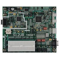
LFEBS12UB Freescale Semiconductor, LFEBS12UB Datasheet - Page 406

LFEBS12UB
Manufacturer Part Number
LFEBS12UB
Description
KIT STUDENT LEARNING S12 DG128
Manufacturer
Freescale Semiconductor
Specifications of LFEBS12UB
Architecture
8/16-bit
Code Gen Tools Included
Code Warrior
Silicon Manufacturer
Freescale
Core Architecture
S12
Core Sub-architecture
S12
Silicon Core Number
MC9S12
Silicon Family Name
S12D
Kit Contents
HCS12 DG128 Learning Kit
Rohs Compliant
Yes
Lead Free Status / RoHS Status
Lead free / RoHS Compliant
- Current page: 406 of 1328
- Download datasheet (9Mb)
BFINSX
Chapter 10 XGATE (S12XGATEV3)
Operation
!(RS1[w:0] ^ RD[w+o:o]) ⇒ RD[w+o:o];
Extracts w+1 bits from register RS1 starting at position 0, performs an XNOR with RD[w+o:o] and writes
the bits back to RD. The remaining bits in RD are not affected. If (o+w) > 15 the upper bits are ignored.
Using R0 as a RS1, this command can be used to toggle bits.
CCR Effects
Code and CPU Cycles
406
N:
Z:
V:
C:
BFINSX RD, RS1, RS2
N
∆
Because of an order from the United States International Trade Commission, BGA-packaged product lines and partnumbers
indicated here currently are not available from Freescale for import or sale in the United States prior to September 2010
Set if bit 15 of the result is set; cleared otherwise.
Set if the result is $0000; cleared otherwise.
0; cleared.
Not affected.
Z
∆
w = (RS2[7:4])
o = (RS2[3:0])
V
0
Source Form
—
C
15
15
15
MC9S12XE-Family Reference Manual , Rev. 1.23
Address
Mode
Bit Field Insert and XNOR
TRI
7
0
1
W4
1
5
W4=3, O4=2
1
4
1
3
3
Machine Code
RD
2
O4
Bit Field Insert XNOR
0
0
0
RS1
RS2
RS1
RD
BFINSX
RS2
Freescale Semiconductor
1
1
Cycles
P
Related parts for LFEBS12UB
Image
Part Number
Description
Manufacturer
Datasheet
Request
R
Part Number:
Description:
Manufacturer:
Freescale Semiconductor, Inc
Datasheet:
Part Number:
Description:
Manufacturer:
Freescale Semiconductor, Inc
Datasheet:
Part Number:
Description:
Manufacturer:
Freescale Semiconductor, Inc
Datasheet:
Part Number:
Description:
Manufacturer:
Freescale Semiconductor, Inc
Datasheet:
Part Number:
Description:
Manufacturer:
Freescale Semiconductor, Inc
Datasheet:
Part Number:
Description:
Manufacturer:
Freescale Semiconductor, Inc
Datasheet:
Part Number:
Description:
Manufacturer:
Freescale Semiconductor, Inc
Datasheet:
Part Number:
Description:
Manufacturer:
Freescale Semiconductor, Inc
Datasheet:
Part Number:
Description:
Manufacturer:
Freescale Semiconductor, Inc
Datasheet:
Part Number:
Description:
Manufacturer:
Freescale Semiconductor, Inc
Datasheet:
Part Number:
Description:
Manufacturer:
Freescale Semiconductor, Inc
Datasheet:
Part Number:
Description:
Manufacturer:
Freescale Semiconductor, Inc
Datasheet:
Part Number:
Description:
Manufacturer:
Freescale Semiconductor, Inc
Datasheet:
Part Number:
Description:
Manufacturer:
Freescale Semiconductor, Inc
Datasheet:
Part Number:
Description:
Manufacturer:
Freescale Semiconductor, Inc
Datasheet:


