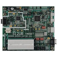
LFEBS12UB Freescale Semiconductor, LFEBS12UB Datasheet - Page 547

LFEBS12UB
Manufacturer Part Number
LFEBS12UB
Description
KIT STUDENT LEARNING S12 DG128
Manufacturer
Freescale Semiconductor
Specifications of LFEBS12UB
Architecture
8/16-bit
Code Gen Tools Included
Code Warrior
Silicon Manufacturer
Freescale
Core Architecture
S12
Core Sub-architecture
S12
Silicon Core Number
MC9S12
Silicon Family Name
S12D
Kit Contents
HCS12 DG128 Learning Kit
Rohs Compliant
Yes
Lead Free Status / RoHS Status
Lead free / RoHS Compliant
- Current page: 547 of 1328
- Download datasheet (9Mb)
14.3.2.12 Main Timer Interrupt Flag 1 (TFLG1)
Read: Anytime
Write used in the flag clearing mechanism. Writing a one to the flag clears the flag. Writing a zero will not
affect the current status of the bit.
All bits reset to zero.
TFLG1 indicates when interrupt conditions have occurred. The flags can be cleared via the normal flag
clearing mechanism (writing a one to the flag) or via the fast flag clearing mechanism (reference TFFCA
bit in
Use of the TFMOD bit in the ICSYS register in conjunction with the use of the ICOVW register allows a
timer interrupt to be generated after capturing two values in the capture and holding registers, instead of
generating an interrupt for every capture.
14.3.2.13 Main Timer Interrupt Flag 2 (TFLG2)
Read: Anytime
Freescale Semiconductor
Module Base + 0x000E
Module Base + 0x000F
Because of an order from the United States International Trade Commission, BGA-packaged product lines and partnumbers
C[7:0]F
Reset
Reset
indicated here currently are not available from Freescale for import or sale in the United States prior to September 2010
Field
7:0
Section 14.3.2.6, “Timer System Control Register 1
W
W
R
R
C7F
Input Capture/Output Compare Channel “x” Flag — A CxF flag is set when a corresponding input capture or
output compare is detected. C0F can also be set by 16-bit Pulse Accumulator B (PACB). C3F–C0F can also be
set by 8-bit pulse accumulators PAC3–PAC0.
If the delay counter is enabled, the CxF flag will not be set until after the delay.
TOF
0
0
7
7
When TFFCA = 1, the flags cannot be cleared via the normal flag clearing
mechanism (writing a one to the flag). Reference
System Control Register 1
= Unimplemented or Reserved
C6F
0
0
0
6
6
Figure 14-18. Main Timer Interrupt Flag 1 (TFLG1)
Figure 14-19. Main Timer Interrupt Flag 2 (TFLG2)
MC9S12XE-Family Reference Manual Rev. 1.23
Table 14-17. TFLG1 Field Descriptions
C5F
5
0
5
0
0
(TSCR1)”.
C4F
NOTE
0
0
0
4
4
Description
(TSCR1)”).
C3F
0
0
0
3
3
Chapter 14 Enhanced Capture Timer (ECT16B8CV3)
Section 14.3.2.6, “Timer
C2F
2
0
2
0
0
C1F
0
0
0
1
1
C0F
0
0
0
0
0
547
Related parts for LFEBS12UB
Image
Part Number
Description
Manufacturer
Datasheet
Request
R
Part Number:
Description:
Manufacturer:
Freescale Semiconductor, Inc
Datasheet:
Part Number:
Description:
Manufacturer:
Freescale Semiconductor, Inc
Datasheet:
Part Number:
Description:
Manufacturer:
Freescale Semiconductor, Inc
Datasheet:
Part Number:
Description:
Manufacturer:
Freescale Semiconductor, Inc
Datasheet:
Part Number:
Description:
Manufacturer:
Freescale Semiconductor, Inc
Datasheet:
Part Number:
Description:
Manufacturer:
Freescale Semiconductor, Inc
Datasheet:
Part Number:
Description:
Manufacturer:
Freescale Semiconductor, Inc
Datasheet:
Part Number:
Description:
Manufacturer:
Freescale Semiconductor, Inc
Datasheet:
Part Number:
Description:
Manufacturer:
Freescale Semiconductor, Inc
Datasheet:
Part Number:
Description:
Manufacturer:
Freescale Semiconductor, Inc
Datasheet:
Part Number:
Description:
Manufacturer:
Freescale Semiconductor, Inc
Datasheet:
Part Number:
Description:
Manufacturer:
Freescale Semiconductor, Inc
Datasheet:
Part Number:
Description:
Manufacturer:
Freescale Semiconductor, Inc
Datasheet:
Part Number:
Description:
Manufacturer:
Freescale Semiconductor, Inc
Datasheet:
Part Number:
Description:
Manufacturer:
Freescale Semiconductor, Inc
Datasheet:


