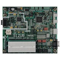
LFEBS12UB Freescale Semiconductor, LFEBS12UB Datasheet - Page 695

LFEBS12UB
Manufacturer Part Number
LFEBS12UB
Description
KIT STUDENT LEARNING S12 DG128
Manufacturer
Freescale Semiconductor
Specifications of LFEBS12UB
Architecture
8/16-bit
Code Gen Tools Included
Code Warrior
Silicon Manufacturer
Freescale
Core Architecture
S12
Core Sub-architecture
S12
Silicon Core Number
MC9S12
Silicon Family Name
S12D
Kit Contents
HCS12 DG128 Learning Kit
Rohs Compliant
Yes
Lead Free Status / RoHS Status
Lead free / RoHS Compliant
- Current page: 695 of 1328
- Download datasheet (9Mb)
19.2.1
This pin serves as waveform output of PWM channel 7 and as an input for the emergency shutdown
feature.
19.2.2
This pin serves as waveform output of PWM channel 6.
19.2.3
This pin serves as waveform output of PWM channel 5.
19.2.4
This pin serves as waveform output of PWM channel 4.
19.2.5
This pin serves as waveform output of PWM channel 3.
19.2.6
This pin serves as waveform output of PWM channel 2.
19.2.7
This pin serves as waveform output of PWM channel 1.
19.2.8
This pin serves as waveform output of PWM channel 0.
19.3
This section describes in detail all the registers and register bits in the PWM module.
The special-purpose registers and register bit functions that are not normally available to device end users,
such as factory test control registers and reserved registers, are clearly identified by means of shading the
appropriate portions of address maps and register diagrams. Notes explaining the reasons for restricting
access to the registers and functions are also explained in the individual register descriptions.
19.3.1
This section describes the content of the registers in the PWM module. The base address of the PWM
module is determined at the MCU level when the MCU is defined. The register decode map is fixed and
begins at the first address of the module address offset. The figure below shows the registers associated
Freescale Semiconductor
Because of an order from the United States International Trade Commission, BGA-packaged product lines and partnumbers
indicated here currently are not available from Freescale for import or sale in the United States prior to September 2010
Memory Map and Register Definition
PWM7 — PWM Channel 7
PWM6 — PWM Channel 6
PWM5 — PWM Channel 5
PWM4 — PWM Channel 4
PWM3 — PWM Channel 3
PWM3 — PWM Channel 2
PWM3 — PWM Channel 1
PWM3 — PWM Channel 0
Module Memory Map
MC9S12XE-Family Reference Manual Rev. 1.23
Chapter 19 Pulse-Width Modulator (S12PWM8B8CV1)
695
Related parts for LFEBS12UB
Image
Part Number
Description
Manufacturer
Datasheet
Request
R
Part Number:
Description:
Manufacturer:
Freescale Semiconductor, Inc
Datasheet:
Part Number:
Description:
Manufacturer:
Freescale Semiconductor, Inc
Datasheet:
Part Number:
Description:
Manufacturer:
Freescale Semiconductor, Inc
Datasheet:
Part Number:
Description:
Manufacturer:
Freescale Semiconductor, Inc
Datasheet:
Part Number:
Description:
Manufacturer:
Freescale Semiconductor, Inc
Datasheet:
Part Number:
Description:
Manufacturer:
Freescale Semiconductor, Inc
Datasheet:
Part Number:
Description:
Manufacturer:
Freescale Semiconductor, Inc
Datasheet:
Part Number:
Description:
Manufacturer:
Freescale Semiconductor, Inc
Datasheet:
Part Number:
Description:
Manufacturer:
Freescale Semiconductor, Inc
Datasheet:
Part Number:
Description:
Manufacturer:
Freescale Semiconductor, Inc
Datasheet:
Part Number:
Description:
Manufacturer:
Freescale Semiconductor, Inc
Datasheet:
Part Number:
Description:
Manufacturer:
Freescale Semiconductor, Inc
Datasheet:
Part Number:
Description:
Manufacturer:
Freescale Semiconductor, Inc
Datasheet:
Part Number:
Description:
Manufacturer:
Freescale Semiconductor, Inc
Datasheet:
Part Number:
Description:
Manufacturer:
Freescale Semiconductor, Inc
Datasheet:


