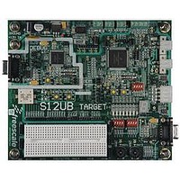
LFEBS12UB Freescale Semiconductor, LFEBS12UB Datasheet - Page 312

LFEBS12UB
Manufacturer Part Number
LFEBS12UB
Description
KIT STUDENT LEARNING S12 DG128
Manufacturer
Freescale Semiconductor
Specifications of LFEBS12UB
Architecture
8/16-bit
Code Gen Tools Included
Code Warrior
Silicon Manufacturer
Freescale
Core Architecture
S12
Core Sub-architecture
S12
Silicon Core Number
MC9S12
Silicon Family Name
S12D
Kit Contents
HCS12 DG128 Learning Kit
Rohs Compliant
Yes
Lead Free Status / RoHS Status
Lead free / RoHS Compliant
- Current page: 312 of 1328
- Download datasheet (9Mb)
Chapter 8 S12X Debug (S12XDBGV3) Module
8.3.2
This section consists of the S12XDBG control and trace buffer register descriptions in address order. Each
comparator has a bank of registers that are visible through an 8-byte window between 0x0028 and 0x002F
in the S12XDBG module register address map. When ARM is set in DBGC1, the only bits in the
S12XDBG module registers that can be written are ARM, TRIG, and COMRV[1:0]
8.3.2.1
Read: Anytime
Write: Bits 7, 1, 0 anytime
312
Address: 0x0020
Because of an order from the United States International Trade Commission, BGA-packaged product lines and partnumbers
Reset
indicated here currently are not available from Freescale for import or sale in the United States prior to September 2010
TRIG
Field
ARM
7
6
W
R
Bit 6 can be written anytime but always reads back as 0.
Bits 5:2 anytime S12XDBG is not armed.
Register Descriptions
ARM
Arm Bit — The ARM bit controls whether the S12XDBG module is armed. This bit can be set and cleared by
user software and is automatically cleared on completion of a tracing session, or if a breakpoint is generated with
tracing not enabled. On setting this bit the state sequencer enters State1.
0 Debugger disarmed
1 Debugger armed
Immediate Trigger Request Bit — This bit when written to 1 requests an immediate trigger independent of
comparator or external tag signal status. When tracing is complete a forced breakpoint may be generated
depending upon DBGBRK and BDM bit settings. This bit always reads back a 0. Writing a 0 to this bit has no
effect. If TSOURCE are clear no tracing is carried out. If tracing has already commenced using BEGIN- or MID
trigger alignment, it continues until the end of the tracing session as defined by the TALIGN bit settings, thus
TRIG has no affect. In secure mode tracing is disabled and writing to this bit has no effect.
0 Do not trigger until the state sequencer enters the Final State.
1 Trigger immediately .
Debug Control Register 1 (DBGC1)
0
7
If a write access to DBGC1 with the ARM bit position set occurs
simultaneously to a hardware disarm from an internal trigger event, then the
ARM bit is cleared due to the hardware disarm.
When disarming the S12XDBG by clearing ARM with software, the
contents of bits[5:2] are not affected by the write, since up until the write
operation, ARM = 1 preventing these bits from being written. These bits
must be cleared using a second write if required.
TRIG
0
0
6
Figure 8-3. Debug Control Register (DBGC1)
MC9S12XE-Family Reference Manual , Rev. 1.23
Table 8-5. DBGC1 Field Descriptions
XGSBPE
5
0
BDM
NOTE
NOTE
0
4
Description
0
3
DBGBRK
2
0
Freescale Semiconductor
0
1
COMRV
0
0
Related parts for LFEBS12UB
Image
Part Number
Description
Manufacturer
Datasheet
Request
R
Part Number:
Description:
Manufacturer:
Freescale Semiconductor, Inc
Datasheet:
Part Number:
Description:
Manufacturer:
Freescale Semiconductor, Inc
Datasheet:
Part Number:
Description:
Manufacturer:
Freescale Semiconductor, Inc
Datasheet:
Part Number:
Description:
Manufacturer:
Freescale Semiconductor, Inc
Datasheet:
Part Number:
Description:
Manufacturer:
Freescale Semiconductor, Inc
Datasheet:
Part Number:
Description:
Manufacturer:
Freescale Semiconductor, Inc
Datasheet:
Part Number:
Description:
Manufacturer:
Freescale Semiconductor, Inc
Datasheet:
Part Number:
Description:
Manufacturer:
Freescale Semiconductor, Inc
Datasheet:
Part Number:
Description:
Manufacturer:
Freescale Semiconductor, Inc
Datasheet:
Part Number:
Description:
Manufacturer:
Freescale Semiconductor, Inc
Datasheet:
Part Number:
Description:
Manufacturer:
Freescale Semiconductor, Inc
Datasheet:
Part Number:
Description:
Manufacturer:
Freescale Semiconductor, Inc
Datasheet:
Part Number:
Description:
Manufacturer:
Freescale Semiconductor, Inc
Datasheet:
Part Number:
Description:
Manufacturer:
Freescale Semiconductor, Inc
Datasheet:
Part Number:
Description:
Manufacturer:
Freescale Semiconductor, Inc
Datasheet:


