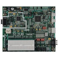
LFEBS12UB Freescale Semiconductor, LFEBS12UB Datasheet - Page 738

LFEBS12UB
Manufacturer Part Number
LFEBS12UB
Description
KIT STUDENT LEARNING S12 DG128
Manufacturer
Freescale Semiconductor
Specifications of LFEBS12UB
Architecture
8/16-bit
Code Gen Tools Included
Code Warrior
Silicon Manufacturer
Freescale
Core Architecture
S12
Core Sub-architecture
S12
Silicon Core Number
MC9S12
Silicon Family Name
S12D
Kit Contents
HCS12 DG128 Learning Kit
Rohs Compliant
Yes
Lead Free Status / RoHS Status
Lead free / RoHS Compliant
- Current page: 738 of 1328
- Download datasheet (9Mb)
Chapter 20 Serial Communication Interface (S12SCIV5)
738
Because of an order from the United States International Trade Commission, BGA-packaged product lines and partnumbers
indicated here currently are not available from Freescale for import or sale in the United States prior to September 2010
Field
OR
NF
FE
PF
3
2
1
0
Overrun Flag — OR is set when software fails to read the SCI data register before the receive shift register
receives the next frame. The OR bit is set immediately after the stop bit has been completely received for the
second frame. The data in the shift register is lost, but the data already in the SCI data registers is not affected.
Clear OR by reading SCI status register 1 (SCISR1) with OR set and then reading SCI data register low
(SCIDRL).
0 No overrun
1 Overrun
Note: OR flag may read back as set when RDRF flag is clear. This may happen if the following sequence of
Noise Flag — NF is set when the SCI detects noise on the receiver input. NF bit is set during the same cycle as
the RDRF flag but does not get set in the case of an overrun. Clear NF by reading SCI status register 1(SCISR1),
and then reading SCI data register low (SCIDRL).
0 No noise
1 Noise
Framing Error Flag — FE is set when a logic 0 is accepted as the stop bit. FE bit is set during the same cycle
as the RDRF flag but does not get set in the case of an overrun. FE inhibits further data reception until it is
cleared. Clear FE by reading SCI status register 1 (SCISR1) with FE set and then reading the SCI data register
low (SCIDRL).
0 No framing error
1 Framing error
Parity Error Flag — PF is set when the parity enable bit (PE) is set and the parity of the received data does not
match the parity type bit (PT). PF bit is set during the same cycle as the RDRF flag but does not get set in the
case of an overrun. Clear PF by reading SCI status register 1 (SCISR1), and then reading SCI data register low
(SCIDRL).
0 No parity error
1 Parity error
events occurs:
Event 3 may be at exactly the same time as event 2 or any time after. When this happens, a dummy
SCIDRL read following event 4 will be required to clear the OR flag if further frames are to be received.
1. After the first frame is received, read status register SCISR1 (returns RDRF set and OR flag clear);
2. Receive second frame without reading the first frame in the data register (the second frame is not
3. Read data register SCIDRL (returns first frame and clears RDRF flag in the status register);
4. Read status register SCISR1 (returns RDRF clear and OR set).
received and OR flag is set);
Table 20-11. SCISR1 Field Descriptions (continued)
MC9S12XE-Family Reference Manual , Rev. 1.23
Description
Freescale Semiconductor
Related parts for LFEBS12UB
Image
Part Number
Description
Manufacturer
Datasheet
Request
R
Part Number:
Description:
Manufacturer:
Freescale Semiconductor, Inc
Datasheet:
Part Number:
Description:
Manufacturer:
Freescale Semiconductor, Inc
Datasheet:
Part Number:
Description:
Manufacturer:
Freescale Semiconductor, Inc
Datasheet:
Part Number:
Description:
Manufacturer:
Freescale Semiconductor, Inc
Datasheet:
Part Number:
Description:
Manufacturer:
Freescale Semiconductor, Inc
Datasheet:
Part Number:
Description:
Manufacturer:
Freescale Semiconductor, Inc
Datasheet:
Part Number:
Description:
Manufacturer:
Freescale Semiconductor, Inc
Datasheet:
Part Number:
Description:
Manufacturer:
Freescale Semiconductor, Inc
Datasheet:
Part Number:
Description:
Manufacturer:
Freescale Semiconductor, Inc
Datasheet:
Part Number:
Description:
Manufacturer:
Freescale Semiconductor, Inc
Datasheet:
Part Number:
Description:
Manufacturer:
Freescale Semiconductor, Inc
Datasheet:
Part Number:
Description:
Manufacturer:
Freescale Semiconductor, Inc
Datasheet:
Part Number:
Description:
Manufacturer:
Freescale Semiconductor, Inc
Datasheet:
Part Number:
Description:
Manufacturer:
Freescale Semiconductor, Inc
Datasheet:
Part Number:
Description:
Manufacturer:
Freescale Semiconductor, Inc
Datasheet:


