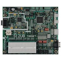
LFEBS12UB Freescale Semiconductor, LFEBS12UB Datasheet - Page 1233

LFEBS12UB
Manufacturer Part Number
LFEBS12UB
Description
KIT STUDENT LEARNING S12 DG128
Manufacturer
Freescale Semiconductor
Specifications of LFEBS12UB
Architecture
8/16-bit
Code Gen Tools Included
Code Warrior
Silicon Manufacturer
Freescale
Core Architecture
S12
Core Sub-architecture
S12
Silicon Core Number
MC9S12
Silicon Family Name
S12D
Kit Contents
HCS12 DG128 Learning Kit
Rohs Compliant
Yes
Lead Free Status / RoHS Status
Lead free / RoHS Compliant
- Current page: 1233 of 1328
- Download datasheet (9Mb)
A.3.2
The reliability of the NVM blocks is guaranteed by stress test during qualification, constant process
monitors and burn-in to screen early life failures.
The data retention and program/erase cycling failure rates are specified at the operating conditions noted.
The program/erase cycle count on the sector is incremented every time a sector or mass erase event is
executed.
The standard shipping condition for both the D-Flash and P-Flash memory is erased with security disabled.
However it is recommended that each block or sector is erased before factory programming to ensure that
the full data retention capability is achieved. Data retention time is measured from the last erase operation.
Freescale Semiconductor
Conditions are shown in
Num C
10
11
12
13
1
2
3
4
5
6
7
8
9
C Data retention at an average junction temperature of T
C Data retention at an average junction temperature of T
C P-Flash number of program/erase cycles
C Data retention at an average junction temperature of T
C Data retention at an average junction temperature of T
C Data retention at an average junction temperature of T
C D-Flash number of program/erase cycles (-40°C ≤ tj ≤ 150°C)
C Data retention at an average junction temperature of T
C Data retention at an average junction temperature of T
C Data retention at an average junction temperature of T
C EEPROM number of program/erase cycles with a ratio of
C EEPROM number of program/erase cycles with a ratio of
C EEPROM number of program/erase cycles with a ratio of
85°C
85°C
(-40°C ≤ tj ≤ 150°C)
85°C
85°C
85°C
85°C
85°C
(e.g. after <20,000 cycles / Spec 100,000 cycles)
85°C
(e.g. after < 200 cycles / Spec 100,000 cycles)
EEE_NVM to EEE_RAM = 8 (-40°C ≤ tj ≤ 150°C)
EEE_NVM to EEE_RAM = 128 (-40°C ≤ tj ≤ 150°C)
EEE_NVM to EEE_RAM = 16384
NVM Reliability Parameters
1
3
3
3
3
1
3
3
after spec. program/erase cycles
after up to 10,000 program/erase cycles
after less than 100 program/erase cycles
after up to 50,000 program/erase cycles
after less than 10,000 program/erase cycles
after less than 100 program/erase cycles
after less than 20% spec.program/erase cycles.
after less than 0.2% spec. program/erase cycles
Table A-4
unless otherwise noted
Table A-20. NVM Reliability Characteristics
MC9S12XE-Family Reference Manual Rev. 1.23
Rating
6
(-40°C ≤ tj ≤ 150°C)
Emulated EEPROM
P-Flash Arrays
D-Flash Array
Javg
Javg
Javg
Javg
Javg
Javg
Javg
Javg
=
=
=
=
=
=
=
=
t
t
t
t
t
t
t
t
EENVMRET
EENVMRET
EENVMRET
Symbol
PNVMRET
PNVMRET
DNVMRET
DNVMRET
DNVMRET
n
n
n
n
n
PFLPE
DFLPE
EEPE
EEPE
EEPE
325M
Appendix A Electrical Characteristics
100K
3M
Min
10K
50K
15
20
10
20
10
20
5
5
4
4
4
4
100K
500K
3.2G
30M
100
100
100
100
100
100
100
100
1M
Typ
5
2
2
2
2
2
2
2
2
5
5
3
3
Max
—
—
—
—
—
—
—
—
—
—
—
—
—
Cycles
Cycles
Cycles
Cycles
Cycles
Years
Years
Years
Years
Years
Years
Years
Years
Unit
1233
Related parts for LFEBS12UB
Image
Part Number
Description
Manufacturer
Datasheet
Request
R
Part Number:
Description:
Manufacturer:
Freescale Semiconductor, Inc
Datasheet:
Part Number:
Description:
Manufacturer:
Freescale Semiconductor, Inc
Datasheet:
Part Number:
Description:
Manufacturer:
Freescale Semiconductor, Inc
Datasheet:
Part Number:
Description:
Manufacturer:
Freescale Semiconductor, Inc
Datasheet:
Part Number:
Description:
Manufacturer:
Freescale Semiconductor, Inc
Datasheet:
Part Number:
Description:
Manufacturer:
Freescale Semiconductor, Inc
Datasheet:
Part Number:
Description:
Manufacturer:
Freescale Semiconductor, Inc
Datasheet:
Part Number:
Description:
Manufacturer:
Freescale Semiconductor, Inc
Datasheet:
Part Number:
Description:
Manufacturer:
Freescale Semiconductor, Inc
Datasheet:
Part Number:
Description:
Manufacturer:
Freescale Semiconductor, Inc
Datasheet:
Part Number:
Description:
Manufacturer:
Freescale Semiconductor, Inc
Datasheet:
Part Number:
Description:
Manufacturer:
Freescale Semiconductor, Inc
Datasheet:
Part Number:
Description:
Manufacturer:
Freescale Semiconductor, Inc
Datasheet:
Part Number:
Description:
Manufacturer:
Freescale Semiconductor, Inc
Datasheet:
Part Number:
Description:
Manufacturer:
Freescale Semiconductor, Inc
Datasheet:


