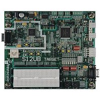
LFEBS12UB Freescale Semiconductor, LFEBS12UB Datasheet - Page 524

LFEBS12UB
Manufacturer Part Number
LFEBS12UB
Description
KIT STUDENT LEARNING S12 DG128
Manufacturer
Freescale Semiconductor
Specifications of LFEBS12UB
Architecture
8/16-bit
Code Gen Tools Included
Code Warrior
Silicon Manufacturer
Freescale
Core Architecture
S12
Core Sub-architecture
S12
Silicon Core Number
MC9S12
Silicon Family Name
S12D
Kit Contents
HCS12 DG128 Learning Kit
Rohs Compliant
Yes
Lead Free Status / RoHS Status
Lead free / RoHS Compliant
- Current page: 524 of 1328
- Download datasheet (9Mb)
Chapter 13 Analog-to-Digital Converter (ADC12B16CV1)
13.3.2.12 ATD Conversion Result Registers (ATDDRn)
The A/D conversion results are stored in 16 result registers. Results are always in unsigned data
representation. Left and right justification is selected using the DJM control bit in ATDCTL3.
If automatic compare of conversions results is enabled (CMPE[n]=1 in ATDCMPE), these registers must
be written with the compare values in left or right justified format depending on the actual value of the
DJM bit. In this case, as the ATDDRn register is used to hold the compare value, the result will not be
stored there at the end of the conversion but is lost.
Read: Anytime
Write: Anytime
13.3.2.12.1 Left Justified Result Data (DJM=0)
13.3.2.12.2 Right Justified Result Data (DJM=1)
Table 13-16
result registers. Compare is always done using all 12 bits of both the conversion result and the compare
value in ATDDRn.
524
Module Base +
0x0010 = ATDDR0, 0x0012 = ATDDR1, 0x0014 = ATDDR2, 0x0016 = ATDDR3
0x0018 = ATDDR4, 0x001A = ATDDR5, 0x001C = ATDDR6, 0x001E = ATDDR7
0x0020 = ATDDR8, 0x0022 = ATDDR9, 0x0024 = ATDDR10, 0x0026 = ATDDR11
0x0028 = ATDDR12, 0x002A = ATDDR13, 0x002C = ATDDR14, 0x002E = ATDDR15
Module Base +
0x0010 = ATDDR0, 0x0012 = ATDDR1, 0x0014 = ATDDR2, 0x0016 = ATDDR3
0x0018 = ATDDR4, 0x001A = ATDDR5, 0x001C = ATDDR6, 0x001E = ATDDR7
0x0020 = ATDDR8, 0x0022 = ATDDR9, 0x0024 = ATDDR10, 0x0026 = ATDDR11
0x0028 = ATDDR12, 0x002A = ATDDR13, 0x002C = ATDDR14, 0x002E = ATDDR15
Because of an order from the United States International Trade Commission, BGA-packaged product lines and partnumbers
Reset
Reset
indicated here currently are not available from Freescale for import or sale in the United States prior to September 2010
W
W
R
R
Bit 11 Bit 10 Bit 9
15
15
0
0
0
shows how depending on the A/D resolution the conversion result is transferred to the ATD
For conversions not using automatic compare, results are stored in the result
registers after each conversion. In this case avoid writing to ATDDRn except
for initial values, because an A/D result might be overwritten.
14
14
0
0
0
Figure 13-15. Right justified ATD conversion result register (ATDDRn)
Figure 13-14. Left justified ATD conversion result register (ATDDRn)
13
13
0
0
0
Bit 8
12
12
0
0
0
MC9S12XE-Family Reference Manual , Rev. 1.23
Bit 11 Bit 10 Bit 9
Bit 7
11
11
0
0
Bit 6
10
10
0
0
Bit 5
0
0
9
9
NOTE
Bit 4
Bit 8
0
0
8
8
Bit 3
Bit 7
0
0
7
7
Bit 2
Bit 6
0
0
6
6
Bit 1
Bit 5
0
0
5
5
Bit 0
Bit 4
0
0
4
4
Bit 3
0
0
0
3
3
Freescale Semiconductor
Bit 2
2
0
0
2
0
Bi1 1
0
0
0
1
1
Bit 0
0
0
0
0
0
Related parts for LFEBS12UB
Image
Part Number
Description
Manufacturer
Datasheet
Request
R
Part Number:
Description:
Manufacturer:
Freescale Semiconductor, Inc
Datasheet:
Part Number:
Description:
Manufacturer:
Freescale Semiconductor, Inc
Datasheet:
Part Number:
Description:
Manufacturer:
Freescale Semiconductor, Inc
Datasheet:
Part Number:
Description:
Manufacturer:
Freescale Semiconductor, Inc
Datasheet:
Part Number:
Description:
Manufacturer:
Freescale Semiconductor, Inc
Datasheet:
Part Number:
Description:
Manufacturer:
Freescale Semiconductor, Inc
Datasheet:
Part Number:
Description:
Manufacturer:
Freescale Semiconductor, Inc
Datasheet:
Part Number:
Description:
Manufacturer:
Freescale Semiconductor, Inc
Datasheet:
Part Number:
Description:
Manufacturer:
Freescale Semiconductor, Inc
Datasheet:
Part Number:
Description:
Manufacturer:
Freescale Semiconductor, Inc
Datasheet:
Part Number:
Description:
Manufacturer:
Freescale Semiconductor, Inc
Datasheet:
Part Number:
Description:
Manufacturer:
Freescale Semiconductor, Inc
Datasheet:
Part Number:
Description:
Manufacturer:
Freescale Semiconductor, Inc
Datasheet:
Part Number:
Description:
Manufacturer:
Freescale Semiconductor, Inc
Datasheet:
Part Number:
Description:
Manufacturer:
Freescale Semiconductor, Inc
Datasheet:


