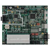
LFEBS12UB Freescale Semiconductor, LFEBS12UB Datasheet - Page 701

LFEBS12UB
Manufacturer Part Number
LFEBS12UB
Description
KIT STUDENT LEARNING S12 DG128
Manufacturer
Freescale Semiconductor
Specifications of LFEBS12UB
Architecture
8/16-bit
Code Gen Tools Included
Code Warrior
Silicon Manufacturer
Freescale
Core Architecture
S12
Core Sub-architecture
S12
Silicon Core Number
MC9S12
Silicon Family Name
S12D
Kit Contents
HCS12 DG128 Learning Kit
Rohs Compliant
Yes
Lead Free Status / RoHS Status
Lead free / RoHS Compliant
- Current page: 701 of 1328
- Download datasheet (9Mb)
19.3.2.3
Each PWM channel has a choice of two clocks to use as the clock source for that channel as described
below.
Read: Anytime
Write: Anytime
Freescale Semiconductor
Module Base + 0x0002
Because of an order from the United States International Trade Commission, BGA-packaged product lines and partnumbers
Reset
PCLK7
PCLK6
PCLK5
PCLK4
PCLK3
PCLK2
PCLK1
PCLK0
indicated here currently are not available from Freescale for import or sale in the United States prior to September 2010
Field
7
6
5
4
3
2
1
0
W
R
PCLK7
Pulse Width Channel 7 Clock Select
0 Clock B is the clock source for PWM channel 7.
1 Clock SB is the clock source for PWM channel 7.
Pulse Width Channel 6 Clock Select
0 Clock B is the clock source for PWM channel 6.
1 Clock SB is the clock source for PWM channel 6.
Pulse Width Channel 5 Clock Select
0 Clock A is the clock source for PWM channel 5.
1 Clock SA is the clock source for PWM channel 5.
Pulse Width Channel 4 Clock Select
0 Clock A is the clock source for PWM channel 4.
1 Clock SA is the clock source for PWM channel 4.
Pulse Width Channel 3 Clock Select
0 Clock B is the clock source for PWM channel 3.
1 Clock SB is the clock source for PWM channel 3.
Pulse Width Channel 2 Clock Select
0 Clock B is the clock source for PWM channel 2.
1 Clock SB is the clock source for PWM channel 2.
Pulse Width Channel 1 Clock Select
0 Clock A is the clock source for PWM channel 1.
1 Clock SA is the clock source for PWM channel 1.
Pulse Width Channel 0 Clock Select
0 Clock A is the clock source for PWM channel 0.
1 Clock SA is the clock source for PWM channel 0.
PWM Clock Select Register (PWMCLK)
0
7
Register bits PCLK0 to PCLK7 can be written anytime. If a clock select is
changed while a PWM signal is being generated, a truncated or stretched
pulse can occur during the transition.
PCLKL6
0
6
Figure 19-5. PWM Clock Select Register (PWMCLK)
MC9S12XE-Family Reference Manual Rev. 1.23
PCLK5
5
0
PCLK4
NOTE
0
4
Description
PCLK3
0
3
Chapter 19 Pulse-Width Modulator (S12PWM8B8CV1)
PCLK2
2
0
PCLK1
0
1
PCLK0
0
0
701
Related parts for LFEBS12UB
Image
Part Number
Description
Manufacturer
Datasheet
Request
R
Part Number:
Description:
Manufacturer:
Freescale Semiconductor, Inc
Datasheet:
Part Number:
Description:
Manufacturer:
Freescale Semiconductor, Inc
Datasheet:
Part Number:
Description:
Manufacturer:
Freescale Semiconductor, Inc
Datasheet:
Part Number:
Description:
Manufacturer:
Freescale Semiconductor, Inc
Datasheet:
Part Number:
Description:
Manufacturer:
Freescale Semiconductor, Inc
Datasheet:
Part Number:
Description:
Manufacturer:
Freescale Semiconductor, Inc
Datasheet:
Part Number:
Description:
Manufacturer:
Freescale Semiconductor, Inc
Datasheet:
Part Number:
Description:
Manufacturer:
Freescale Semiconductor, Inc
Datasheet:
Part Number:
Description:
Manufacturer:
Freescale Semiconductor, Inc
Datasheet:
Part Number:
Description:
Manufacturer:
Freescale Semiconductor, Inc
Datasheet:
Part Number:
Description:
Manufacturer:
Freescale Semiconductor, Inc
Datasheet:
Part Number:
Description:
Manufacturer:
Freescale Semiconductor, Inc
Datasheet:
Part Number:
Description:
Manufacturer:
Freescale Semiconductor, Inc
Datasheet:
Part Number:
Description:
Manufacturer:
Freescale Semiconductor, Inc
Datasheet:
Part Number:
Description:
Manufacturer:
Freescale Semiconductor, Inc
Datasheet:


