Z8FMC160100KITG Zilog, Z8FMC160100KITG Datasheet - Page 161
Z8FMC160100KITG
Manufacturer Part Number
Z8FMC160100KITG
Description
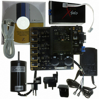
KIT DEV FOR Z8 ENCORE Z8FMC16100
Manufacturer
Zilog
Series
Z8 Encore! MC™r
Datasheets
1.Z8FMC160100KIT.pdf
(7 pages)
2.Z8FMC160100KIT.pdf
(383 pages)
3.Z8FMC160100KITG.pdf
(2 pages)
4.Z8FMC160100KITG.pdf
(15 pages)
Specifications of Z8FMC160100KITG
Main Purpose
Power Management, Motor Control
Embedded
Yes, MCU, 8-Bit
Utilized Ic / Part
Z8FMC16100
Primary Attributes
3-Ph DC Motors
Secondary Attributes
Graphical User Interface
For Use With
269-4664 - KIT ACC OPTO-ISO USB SMART CABLE269-4661 - KIT ACC ETHERNET SMART CABLE269-4539 - KIT ACCESSORY USB SMART CABLE
Lead Free Status / RoHS Status
Lead free / RoHS Compliant
Other names
269-4660


PS024613-0910
Operation
SPI Signals
The SPI is a full-duplex, synchronous, character-oriented channel that supports a four-wire
interface (serial clock, transmit, receive, and slave select). The SPI block consists of a
transmit/receive shift register, a Baud Rate (clock) Generator, and a control unit.
During an SPI transfer, data is sent and received simultaneously by both the master and the
slave SPI devices. Separate signals are required for data and the serial clock. When an SPI
transfer occurs, a multibit (typically 8-bit) character is shifted out one data pin and an
multibit character is simultaneously shifted in on a second data pin. An 8-bit shift register
in the master and another 8-bit shift register in the slave are connected as a circular buffer.
The SPI shift register is single-buffered in the transmit and receive directions. New data to
be transmitted cannot be written into the shift register until the previous transmission is
complete and receive data (if valid) has been read.
The four basic SPI signals are:
•
•
•
•
Each signal is described in both MASTER and SLAVE modes.
Master-In/Slave-Out
The Master-In/Slave-Out (MISO) pin is configured as an input in a master device and as an
output in a slave device. It is one of the two lines that transfer serial data, with the most sig-
nificant bit sent first. The MISO pin of a slave device is placed in a high-impedance state if
the slave is not selected. When the SPI is not enabled, this signal is in a high-impedance
state.
Master-Out/Slave-In
The Master-Out/Slave-In (MOSI) pin is configured as an output in a master device and as
an input in a slave device. It is one of the two lines that transfer serial data, with the most
significant bit sent first. When the SPI is not enabled, this signal is in a high-impedance
state.
Serial Clock
The Serial Clock (SCK) synchronizes data movement both in and out of the device through
its MOSI and MISO pins. In MASTER mode, the SPI’s Baud Rate Generator creates the
Master-In/Slave-Out (MISO)
Master-Out/Slave-In (MOSI)
Serial Clock (SCK)
Slave Select (SS)
Z8FMC16100 Series Flash MCU
Product Specification
Operation
149
Related parts for Z8FMC160100KITG
Image
Part Number
Description
Manufacturer
Datasheet
Request
R

Part Number:
Description:
Communication Controllers, ZILOG INTELLIGENT PERIPHERAL CONTROLLER (ZIP)
Manufacturer:
Zilog, Inc.
Datasheet:

Part Number:
Description:
KIT DEV FOR Z8 ENCORE 16K TO 64K
Manufacturer:
Zilog
Datasheet:

Part Number:
Description:
KIT DEV Z8 ENCORE XP 28-PIN
Manufacturer:
Zilog
Datasheet:

Part Number:
Description:
DEV KIT FOR Z8 ENCORE 8K/4K
Manufacturer:
Zilog
Datasheet:

Part Number:
Description:
KIT DEV Z8 ENCORE XP 28-PIN
Manufacturer:
Zilog
Datasheet:

Part Number:
Description:
DEV KIT FOR Z8 ENCORE 4K TO 8K
Manufacturer:
Zilog
Datasheet:
Part Number:
Description:
CMOS Z8 microcontroller. ROM 16 Kbytes, RAM 256 bytes, speed 16 MHz, 32 lines I/O, 3.0V to 5.5V
Manufacturer:
Zilog, Inc.
Datasheet:
Part Number:
Description:
Low-cost microcontroller. 512 bytes ROM, 61 bytes RAM, 8 MHz
Manufacturer:
Zilog, Inc.
Datasheet:
Part Number:
Description:
Z8 4K OTP Microcontroller
Manufacturer:
Zilog, Inc.
Datasheet:
Part Number:
Description:
CMOS SUPER8 ROMLESS MCU
Manufacturer:
Zilog, Inc.
Datasheet:
Part Number:
Description:
SL1866 CMOSZ8 OTP Microcontroller
Manufacturer:
Zilog, Inc.
Datasheet:
Part Number:
Description:
SL1866 CMOSZ8 OTP Microcontroller
Manufacturer:
Zilog, Inc.
Datasheet:
Part Number:
Description:
OTP (KB) = 1, RAM = 125, Speed = 12, I/O = 14, 8-bit Timers = 2, Comm Interfaces Other Features = Por, LV Protect, Voltage = 4.5-5.5V
Manufacturer:
Zilog, Inc.
Datasheet:
Part Number:
Description:
Manufacturer:
Zilog, Inc.
Datasheet: