Z8FMC160100KITG Zilog, Z8FMC160100KITG Datasheet - Page 202
Z8FMC160100KITG
Manufacturer Part Number
Z8FMC160100KITG
Description
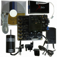
KIT DEV FOR Z8 ENCORE Z8FMC16100
Manufacturer
Zilog
Series
Z8 Encore! MC™r
Datasheets
1.Z8FMC160100KIT.pdf
(7 pages)
2.Z8FMC160100KIT.pdf
(383 pages)
3.Z8FMC160100KITG.pdf
(2 pages)
4.Z8FMC160100KITG.pdf
(15 pages)
Specifications of Z8FMC160100KITG
Main Purpose
Power Management, Motor Control
Embedded
Yes, MCU, 8-Bit
Utilized Ic / Part
Z8FMC16100
Primary Attributes
3-Ph DC Motors
Secondary Attributes
Graphical User Interface
For Use With
269-4664 - KIT ACC OPTO-ISO USB SMART CABLE269-4661 - KIT ACC ETHERNET SMART CABLE269-4539 - KIT ACCESSORY USB SMART CABLE
Lead Free Status / RoHS Status
Lead free / RoHS Compliant
Other names
269-4660


Table 101. I
BITS
FIELD
RESET
R/W
ADDR
PS024613-0910
I
Reserved
2
C Mode Register
2
C Mode Register (I2CMODE)
R
7
0
The I
mode, slave address, and diagnostic modes.
MODE—Selects the I
00 = Master/Slave capable (supports multi-Master arbitration) with 7-bit Slave address
01 = Master/Slave capable (supports multi-Master arbitration) with 10-bit Slave address
10 = Slave Only capable with 7-bit address
11 = Slave Only capable with 10-bit address
IRM—Interactive Receive Mode
Valid in Slave mode when software needs to interpret each received byte before acknowl-
edging. This bit is useful for processing the data bytes following a General Call Address or
if software wants to disable hardware address recognition.
0 = Acknowledge occurs automatically and is determined by the value of the
the I2CCTL register.
1 = A receive interrupt is generated for each byte received (address or data). The SCL is
held Low during the acknowledge cycle until software writes to the I2CCTL register. The
value written to the
software to Acknowledge or Not Acknowledge after interpreting the associated address/
data byte.
GCE—General Call Address Enable
Enables reception of messages beginning with the General Call Address or START byte.
0 = Do not accept a message with the General Call Address or START byte.
1 = Do accept a message with the General Call Address or START byte. When an address
match occurs, the GCA and RD bits in the I
address matched the General Call Address/START byte or not. Following the General Call
Address byte, software may set the
data byte(s) before acknowledging.
SLA[9:8]— Slave Address Bits 9 and 8
Initialize with the appropriate Slave address value when using 10-bit Slave addressing.
These bits are ignored when using 7-bit Slave addressing.
2
C Mode register
6
MODE[1:0]
R/W
0
NAK
2
5
(Table
C Controller operational mode
bit of the I2CCTL register is output on SDA. This value allows
101) provides control over master versus slave operating
R/W
IRM
4
0
IRM
F56H
bit that allows software to examine the following
GCE
R/W
2
3
0
C Status register indicates whether the
Z8FMC16100 Series Flash MCU
2
SLA[9:8]
R/W
Product Specification
0
1
I
2
C Mode Register
NAK
DIAG
R/W
0
0
bit of
190
Related parts for Z8FMC160100KITG
Image
Part Number
Description
Manufacturer
Datasheet
Request
R

Part Number:
Description:
Communication Controllers, ZILOG INTELLIGENT PERIPHERAL CONTROLLER (ZIP)
Manufacturer:
Zilog, Inc.
Datasheet:

Part Number:
Description:
KIT DEV FOR Z8 ENCORE 16K TO 64K
Manufacturer:
Zilog
Datasheet:

Part Number:
Description:
KIT DEV Z8 ENCORE XP 28-PIN
Manufacturer:
Zilog
Datasheet:

Part Number:
Description:
DEV KIT FOR Z8 ENCORE 8K/4K
Manufacturer:
Zilog
Datasheet:

Part Number:
Description:
KIT DEV Z8 ENCORE XP 28-PIN
Manufacturer:
Zilog
Datasheet:

Part Number:
Description:
DEV KIT FOR Z8 ENCORE 4K TO 8K
Manufacturer:
Zilog
Datasheet:
Part Number:
Description:
CMOS Z8 microcontroller. ROM 16 Kbytes, RAM 256 bytes, speed 16 MHz, 32 lines I/O, 3.0V to 5.5V
Manufacturer:
Zilog, Inc.
Datasheet:
Part Number:
Description:
Low-cost microcontroller. 512 bytes ROM, 61 bytes RAM, 8 MHz
Manufacturer:
Zilog, Inc.
Datasheet:
Part Number:
Description:
Z8 4K OTP Microcontroller
Manufacturer:
Zilog, Inc.
Datasheet:
Part Number:
Description:
CMOS SUPER8 ROMLESS MCU
Manufacturer:
Zilog, Inc.
Datasheet:
Part Number:
Description:
SL1866 CMOSZ8 OTP Microcontroller
Manufacturer:
Zilog, Inc.
Datasheet:
Part Number:
Description:
SL1866 CMOSZ8 OTP Microcontroller
Manufacturer:
Zilog, Inc.
Datasheet:
Part Number:
Description:
OTP (KB) = 1, RAM = 125, Speed = 12, I/O = 14, 8-bit Timers = 2, Comm Interfaces Other Features = Por, LV Protect, Voltage = 4.5-5.5V
Manufacturer:
Zilog, Inc.
Datasheet:
Part Number:
Description:
Manufacturer:
Zilog, Inc.
Datasheet: