Z8FMC160100KITG Zilog, Z8FMC160100KITG Datasheet - Page 177
Z8FMC160100KITG
Manufacturer Part Number
Z8FMC160100KITG
Description
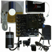
KIT DEV FOR Z8 ENCORE Z8FMC16100
Manufacturer
Zilog
Series
Z8 Encore! MC™r
Datasheets
1.Z8FMC160100KIT.pdf
(7 pages)
2.Z8FMC160100KIT.pdf
(383 pages)
3.Z8FMC160100KITG.pdf
(2 pages)
4.Z8FMC160100KITG.pdf
(15 pages)
Specifications of Z8FMC160100KITG
Main Purpose
Power Management, Motor Control
Embedded
Yes, MCU, 8-Bit
Utilized Ic / Part
Z8FMC16100
Primary Attributes
3-Ph DC Motors
Secondary Attributes
Graphical User Interface
For Use With
269-4664 - KIT ACC OPTO-ISO USB SMART CABLE269-4661 - KIT ACC ETHERNET SMART CABLE269-4539 - KIT ACCESSORY USB SMART CABLE
Lead Free Status / RoHS Status
Lead free / RoHS Compliant
Other names
269-4660


PS024613-0910
I
2
C Interrupts
The I
request signal to the interrupt controller. If the I
interrupt is determined by which bits are set in the I2CISTAT register. If the I
controller is disabled, the BRG controller can be used to generate general-purpose timer
interrupts.
Each interrupt source, other than the baud rate generator interrupt, features an associated
bit in the I2CISTAT register that clears automatically when software reads the register or
performs another task, such as reading/writing the data register.
Transmit Interrupts
Transmit interrupts (
of which must be true:
•
•
Writing to the I
Receive Interrupts
Receive interrupts (
received by the I
register. If the RDRF interrupt is not serviced prior to the completion of the next Receive
byte, the I
RDRF
slave receives an address byte or for data bytes following a slave address that did not
match. An exception is if the Interactive Receive Mode (
register, in which case Receive interrupts occur for all Receive address and data bytes in
SLAVE mode.
Slave Address Match Interrupts
Slave address match interrupts (
in SLAVE mode and an address is received that matches the unique slave address. The
General Call Address (
GCE
register to determine if the transaction is a Read or Write transaction. The General Call
Address and STARTBYTE address are also distinguished by the
Address (
The transmit data register is empty and the
The I
–
–
–
bit = 1 in the I2CMODE register. The software checks the
2
is cleared, to prevent receive overruns. A receive interrupt does not occur when a
C controller contains multiple interrupt sources that are combined into one interrupt
The first bit of a 10-bit address is shifted out
The first bit of the final byte of an address is shifted out and the
deasserted
The first bit of a data byte is shifted out
2
GCA
C controller is enabled, with one of the following:
2
C controller holds SCL Low during the final data bit of the next byte until
) bit of the I2CISTAT register indicates whether the address match occurred
2
C Data register always clears the
2
C controller. The
TDRE
RDRF
0000_0000
bit = 1 in I2CISTAT) occur under the following conditions, both
bit = 1 in I2CISTAT) occur when a byte of data has been
SAM
) and STARTBYTE (
bit = 1 in I2CISTAT) occur when the I
RDRF
bit is cleared by reading from the I
TXI
2
C controller is enabled, the source of the
TRDE
bit = 1 in the I
Z8FMC16100 Series Flash MCU
bit to 0.
0000_0001
IRM
) bit is set in the I2CMODE
Product Specification
RD
RD
2
C Control register
) are recognized if the
bit. The General Call
bit in the I2CISTAT
RD
2
bit is
C controller is
2
I
C
2
C Interrupts
2
C Data
165
Related parts for Z8FMC160100KITG
Image
Part Number
Description
Manufacturer
Datasheet
Request
R

Part Number:
Description:
Communication Controllers, ZILOG INTELLIGENT PERIPHERAL CONTROLLER (ZIP)
Manufacturer:
Zilog, Inc.
Datasheet:

Part Number:
Description:
KIT DEV FOR Z8 ENCORE 16K TO 64K
Manufacturer:
Zilog
Datasheet:

Part Number:
Description:
KIT DEV Z8 ENCORE XP 28-PIN
Manufacturer:
Zilog
Datasheet:

Part Number:
Description:
DEV KIT FOR Z8 ENCORE 8K/4K
Manufacturer:
Zilog
Datasheet:

Part Number:
Description:
KIT DEV Z8 ENCORE XP 28-PIN
Manufacturer:
Zilog
Datasheet:

Part Number:
Description:
DEV KIT FOR Z8 ENCORE 4K TO 8K
Manufacturer:
Zilog
Datasheet:
Part Number:
Description:
CMOS Z8 microcontroller. ROM 16 Kbytes, RAM 256 bytes, speed 16 MHz, 32 lines I/O, 3.0V to 5.5V
Manufacturer:
Zilog, Inc.
Datasheet:
Part Number:
Description:
Low-cost microcontroller. 512 bytes ROM, 61 bytes RAM, 8 MHz
Manufacturer:
Zilog, Inc.
Datasheet:
Part Number:
Description:
Z8 4K OTP Microcontroller
Manufacturer:
Zilog, Inc.
Datasheet:
Part Number:
Description:
CMOS SUPER8 ROMLESS MCU
Manufacturer:
Zilog, Inc.
Datasheet:
Part Number:
Description:
SL1866 CMOSZ8 OTP Microcontroller
Manufacturer:
Zilog, Inc.
Datasheet:
Part Number:
Description:
SL1866 CMOSZ8 OTP Microcontroller
Manufacturer:
Zilog, Inc.
Datasheet:
Part Number:
Description:
OTP (KB) = 1, RAM = 125, Speed = 12, I/O = 14, 8-bit Timers = 2, Comm Interfaces Other Features = Por, LV Protect, Voltage = 4.5-5.5V
Manufacturer:
Zilog, Inc.
Datasheet:
Part Number:
Description:
Manufacturer:
Zilog, Inc.
Datasheet: