Z8FMC160100KITG Zilog, Z8FMC160100KITG Datasheet - Page 176
Z8FMC160100KITG
Manufacturer Part Number
Z8FMC160100KITG
Description
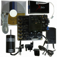
KIT DEV FOR Z8 ENCORE Z8FMC16100
Manufacturer
Zilog
Series
Z8 Encore! MC™r
Datasheets
1.Z8FMC160100KIT.pdf
(7 pages)
2.Z8FMC160100KIT.pdf
(383 pages)
3.Z8FMC160100KITG.pdf
(2 pages)
4.Z8FMC160100KITG.pdf
(15 pages)
Specifications of Z8FMC160100KITG
Main Purpose
Power Management, Motor Control
Embedded
Yes, MCU, 8-Bit
Utilized Ic / Part
Z8FMC16100
Primary Attributes
3-Ph DC Motors
Secondary Attributes
Graphical User Interface
For Use With
269-4664 - KIT ACC OPTO-ISO USB SMART CABLE269-4661 - KIT ACC ETHERNET SMART CABLE269-4539 - KIT ACCESSORY USB SMART CABLE
Lead Free Status / RoHS Status
Lead free / RoHS Compliant
Other names
269-4660


PS024613-0910
Operation
SDA and SCL Signals
•
•
The I
mode, or with master arbitration. In MASTER/SLAVE mode, it can be used as the only
master on the bus or as one of several masters on the bus, with arbitration. In a multimaster
environment, the controller switches from MASTER to SLAVE mode upon losing
arbitration.
Though slave operation is fully supported in MASTER/SLAVE mode, if a device is
intended to operate only as a slave, then SLAVE ONLY mode can be selected. In SLAVE
ONLY mode, the device will not initiate a transaction, even if the software inadvertently
sets the START bit.
The I
most-significant bit first. SCL is the clock for the I
alternate functions are selected for their respective GPIO ports, the pins are automatically
configured for open-drain operation.
The master is responsible for driving the SCL clock signal. During Low period of the
clock, a slave can hold the SCL signal Low to suspend the transaction if it is not ready to
proceed. The master releases the clock at the end of the Low period and notices that the
clock remains Low instead of returning to a High level. When the slave releases the clock,
the I
amount of data transferred in one operation. When transmitting address, data, or an
Acknowledge, the SDA signal changes in the middle of the Low period of SCL
receiving address, Data or an Acknowledge, the SDA signal is sampled in the middle of
the High period of SCL.
A low-pass digital filter can be applied to the SDA and SCL receive signals by setting the
Filter Enable (
glitch less than a system clock period in width will be rejected. This filter should be
enabled when running in I
rates.
The ACKV bit in the I2CSTATE register enables the master to check the Acknowledge
from the slave before sending the next byte.
Support for multimaster environments—if arbitration is lost when operating as a
master, the ARBLST bit in the I2CISTAT register is set and the mode automatically
switches to SLAVE mode.
2
C master continues transaction. All data is transferred in bytes; there is no limit to the
2
2
C Master/Slave Controller operates in MASTER/SLAVE mode, SLAVE ONLY
C circuit sends all addresses, data, and acknowledges signals over the SDA line,
FILTEN
) bit in the I
2
C FAST mode (400 kbps), and can also be used at lower data
2
C Control register. When the filter is enabled, any
2
Z8FMC16100 Series Flash MCU
C bus. When the SDA and SCL pin
Product Specification
Operation
.
When
164
Related parts for Z8FMC160100KITG
Image
Part Number
Description
Manufacturer
Datasheet
Request
R

Part Number:
Description:
Communication Controllers, ZILOG INTELLIGENT PERIPHERAL CONTROLLER (ZIP)
Manufacturer:
Zilog, Inc.
Datasheet:

Part Number:
Description:
KIT DEV FOR Z8 ENCORE 16K TO 64K
Manufacturer:
Zilog
Datasheet:

Part Number:
Description:
KIT DEV Z8 ENCORE XP 28-PIN
Manufacturer:
Zilog
Datasheet:

Part Number:
Description:
DEV KIT FOR Z8 ENCORE 8K/4K
Manufacturer:
Zilog
Datasheet:

Part Number:
Description:
KIT DEV Z8 ENCORE XP 28-PIN
Manufacturer:
Zilog
Datasheet:

Part Number:
Description:
DEV KIT FOR Z8 ENCORE 4K TO 8K
Manufacturer:
Zilog
Datasheet:
Part Number:
Description:
CMOS Z8 microcontroller. ROM 16 Kbytes, RAM 256 bytes, speed 16 MHz, 32 lines I/O, 3.0V to 5.5V
Manufacturer:
Zilog, Inc.
Datasheet:
Part Number:
Description:
Low-cost microcontroller. 512 bytes ROM, 61 bytes RAM, 8 MHz
Manufacturer:
Zilog, Inc.
Datasheet:
Part Number:
Description:
Z8 4K OTP Microcontroller
Manufacturer:
Zilog, Inc.
Datasheet:
Part Number:
Description:
CMOS SUPER8 ROMLESS MCU
Manufacturer:
Zilog, Inc.
Datasheet:
Part Number:
Description:
SL1866 CMOSZ8 OTP Microcontroller
Manufacturer:
Zilog, Inc.
Datasheet:
Part Number:
Description:
SL1866 CMOSZ8 OTP Microcontroller
Manufacturer:
Zilog, Inc.
Datasheet:
Part Number:
Description:
OTP (KB) = 1, RAM = 125, Speed = 12, I/O = 14, 8-bit Timers = 2, Comm Interfaces Other Features = Por, LV Protect, Voltage = 4.5-5.5V
Manufacturer:
Zilog, Inc.
Datasheet:
Part Number:
Description:
Manufacturer:
Zilog, Inc.
Datasheet: