Z8FMC160100KITG Zilog, Z8FMC160100KITG Datasheet - Page 79
Z8FMC160100KITG
Manufacturer Part Number
Z8FMC160100KITG
Description
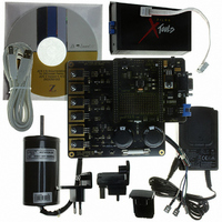
KIT DEV FOR Z8 ENCORE Z8FMC16100
Manufacturer
Zilog
Series
Z8 Encore! MC™r
Datasheets
1.Z8FMC160100KIT.pdf
(7 pages)
2.Z8FMC160100KIT.pdf
(383 pages)
3.Z8FMC160100KITG.pdf
(2 pages)
4.Z8FMC160100KITG.pdf
(15 pages)
Specifications of Z8FMC160100KITG
Main Purpose
Power Management, Motor Control
Embedded
Yes, MCU, 8-Bit
Utilized Ic / Part
Z8FMC16100
Primary Attributes
3-Ph DC Motors
Secondary Attributes
Graphical User Interface
For Use With
269-4664 - KIT ACC OPTO-ISO USB SMART CABLE269-4661 - KIT ACC ETHERNET SMART CABLE269-4539 - KIT ACCESSORY USB SMART CABLE
Lead Free Status / RoHS Status
Lead free / RoHS Compliant
Other names
269-4660


PS024613-0910
PWM Off State and Output Polarity
PWM Channel Pair Enable
PWM Reload Event
The default OFF state and the polarity of the PWM outputs are controlled by the
and
PWM High outputs H0, H1, and H2. The
polarity for the Low outputs L0, L1, and L2.
The OFF state is the value programmed in the option bit. For example, programming
PWMHI
active state a Low logic value. Conversely, programming
state to be a Low logic value.
The relative polarity of the PWM channel pairs is controlled by the
Control 1 register (PWMCTL1). These bits do not affect the OFF state programmed by the
option bits. Setting these bits inverts the High and Low of the selected channels. The relative
channel polarity controls the order in which the signals of a given PWM pair toggle. If a
bit is reset to zero, the High will first go active at the start of a PWM period. Alternately, if the
bit is set, the Low will go active first. A switching of the
PWM reload event (see below). In complementary mode, the switch is additionally delayed
until the end of the programmed deadband time.
Following a POR, the PWM pins enter a high-impedance state. As the internal reset pro-
ceeds, the PWM outputs are forced to the OFF state as determined by the
PWMLO
The
output pairs, respectively. If a PWM channel pair is not enabled, it remains in a high-
impedance state after reset and can be used as a general-purpose input.
To prevent erroneous PWM pulse-widths and periods, registers that control the timing of the
output are buffered. Buffering causes all of the PWM compare values to update at the same
time. In other words, the registers that control the duty cycle and clock source prescaler only
take effect upon a PWM reload event. A PWM reload event can be configured to occur at
the end of each PWM period, or only every 2, 4, or 8 PWM periods by setting the RELFREQ
bits in the PWM Control 1 register (PWMCTL1). The software must indicate that all new
values are ready by setting the READY bit in the PWM Control 0 register (PWMCTL0) to 1.
After this READY bit has been set to 1, the buffered values take effect at the next reload
event.
PWMLO
PWM0EN
OFF state option bits.
to a 1 sets the OFF state of PWMH0, H1, and H2 to a High logic value and the
option bits. The
,
PWM1EN
, and
PWMHI
PWM2EN
PWMLO
option controls the OFF state and the polarity for the
is programmed in a similar manner.
option bits enable the PWM0, PWM1, and PWM2
PWMLO
option controls the OFF state and the
Z8FMC16100 Series Flash MCU
POL
PWM Off State and Output Polarity
PWMHI
x bits is synchronized with the
Product Specification
to a 0 causes the OFF
POL
x bits in the PWM
PWMHI
PWMHI
POL
and
x
67
Related parts for Z8FMC160100KITG
Image
Part Number
Description
Manufacturer
Datasheet
Request
R

Part Number:
Description:
Communication Controllers, ZILOG INTELLIGENT PERIPHERAL CONTROLLER (ZIP)
Manufacturer:
Zilog, Inc.
Datasheet:

Part Number:
Description:
KIT DEV FOR Z8 ENCORE 16K TO 64K
Manufacturer:
Zilog
Datasheet:

Part Number:
Description:
KIT DEV Z8 ENCORE XP 28-PIN
Manufacturer:
Zilog
Datasheet:

Part Number:
Description:
DEV KIT FOR Z8 ENCORE 8K/4K
Manufacturer:
Zilog
Datasheet:

Part Number:
Description:
KIT DEV Z8 ENCORE XP 28-PIN
Manufacturer:
Zilog
Datasheet:

Part Number:
Description:
DEV KIT FOR Z8 ENCORE 4K TO 8K
Manufacturer:
Zilog
Datasheet:
Part Number:
Description:
CMOS Z8 microcontroller. ROM 16 Kbytes, RAM 256 bytes, speed 16 MHz, 32 lines I/O, 3.0V to 5.5V
Manufacturer:
Zilog, Inc.
Datasheet:
Part Number:
Description:
Low-cost microcontroller. 512 bytes ROM, 61 bytes RAM, 8 MHz
Manufacturer:
Zilog, Inc.
Datasheet:
Part Number:
Description:
Z8 4K OTP Microcontroller
Manufacturer:
Zilog, Inc.
Datasheet:
Part Number:
Description:
CMOS SUPER8 ROMLESS MCU
Manufacturer:
Zilog, Inc.
Datasheet:
Part Number:
Description:
SL1866 CMOSZ8 OTP Microcontroller
Manufacturer:
Zilog, Inc.
Datasheet:
Part Number:
Description:
SL1866 CMOSZ8 OTP Microcontroller
Manufacturer:
Zilog, Inc.
Datasheet:
Part Number:
Description:
OTP (KB) = 1, RAM = 125, Speed = 12, I/O = 14, 8-bit Timers = 2, Comm Interfaces Other Features = Por, LV Protect, Voltage = 4.5-5.5V
Manufacturer:
Zilog, Inc.
Datasheet:
Part Number:
Description:
Manufacturer:
Zilog, Inc.
Datasheet: