Z8FMC160100KITG Zilog, Z8FMC160100KITG Datasheet - Page 189
Z8FMC160100KITG
Manufacturer Part Number
Z8FMC160100KITG
Description
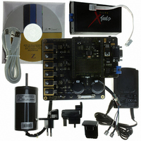
KIT DEV FOR Z8 ENCORE Z8FMC16100
Manufacturer
Zilog
Series
Z8 Encore! MC™r
Datasheets
1.Z8FMC160100KIT.pdf
(7 pages)
2.Z8FMC160100KIT.pdf
(383 pages)
3.Z8FMC160100KITG.pdf
(2 pages)
4.Z8FMC160100KITG.pdf
(15 pages)
Specifications of Z8FMC160100KITG
Main Purpose
Power Management, Motor Control
Embedded
Yes, MCU, 8-Bit
Utilized Ic / Part
Z8FMC16100
Primary Attributes
3-Ph DC Motors
Secondary Attributes
Graphical User Interface
For Use With
269-4664 - KIT ACC OPTO-ISO USB SMART CABLE269-4661 - KIT ACC ETHERNET SMART CABLE269-4539 - KIT ACCESSORY USB SMART CABLE
Lead Free Status / RoHS Status
Lead free / RoHS Compliant
Other names
269-4660


PS024613-0910
S
Slave Address
Figure 32. Data Transfer Format—Slave Receive Transaction with 7-Bit Address
Slave Receive Transaction with 7-Bit Address
The data transfer format for writing data from a master to a slave in 7-bit address mode is
shown in
operating as a slave in 7-bit addressing mode and receiving data from the bus master.
1. The software configures the controller for operation as a slave in 7-bit addressing
2. The bus master initiates a transfer, sending the address byte. In SLAVE mode, the I
3. The software responds to the interrupt by reading the I2CISTAT register (which clears
4. The master detects the Acknowledge and sends the byte of data.
5. The I
6. The software responds by reading the I2CISTAT register, finding the
7. The master and slave loops through steps 4 to 6 until the master detects a Not
mode, as follows:
(a) Initialize the
(b) Optionally set the
(c) Initialize the
(d) Set
controller recognizes its own address and detects that the R/W bit = 0 (written from
the master to the slave). The I
accept the transaction. The
interrupt. The
slave. The I
the first data byte.
the
= 0, no immediate action is required until the first byte of data is received. If software
is only able to accept a single byte it sets the
time.
Acknowledge depending on the state of the
controller generates the receive data interrupt by setting the
register.
reading the I2CDATA register clearing the
more data byte it sets the
Acknowledge instruction or runs out of data to send.
SAM
or MASTER/SLAVE mode with 7-bit addressing.
2
Figure
C controller receives the data byte and responds with Acknowledge or Not
IEN
bit). After seeing the
W=0
2
= 1 in the I
C controller holds the SCL signal Low, waiting for the software to load
32. The procedure that follows describes the I
RD
MODE
SLA[6:0]
bit in the I2CISTAT register is cleared to 0, indicating a Write to the
A
GCE
field in the I
2
C Control register. Set
NAK
bit.
SAM
bits in the I
Data
SAM
2
bit in the I2CCTL register.
C controller acknowledges, indicating it is available to
bit in the I2CISTAT register is set to 1, causing an
bit to 1, the software checks the
2
C Mode register for either SLAVE ONLY mode
A
2
C Slave Address register.
RDRF
NAK
NAK
Data
NAK
bit in the I2CCTL register. The I
Z8FMC16100 Series Flash MCU
bit. If software can accept only one
bit in the I2CCTL register at this
= 0 in the I
A
2
C Master/Slave Controller
RDRF
Product Specification
Data
2
C Control register.
bit in the I2CISTAT
RD
Slave Transactions
RDRF
bit. Because
A/A
bit = 1 and
P/S
2
C
2
RD
C
177
Related parts for Z8FMC160100KITG
Image
Part Number
Description
Manufacturer
Datasheet
Request
R

Part Number:
Description:
Communication Controllers, ZILOG INTELLIGENT PERIPHERAL CONTROLLER (ZIP)
Manufacturer:
Zilog, Inc.
Datasheet:

Part Number:
Description:
KIT DEV FOR Z8 ENCORE 16K TO 64K
Manufacturer:
Zilog
Datasheet:

Part Number:
Description:
KIT DEV Z8 ENCORE XP 28-PIN
Manufacturer:
Zilog
Datasheet:

Part Number:
Description:
DEV KIT FOR Z8 ENCORE 8K/4K
Manufacturer:
Zilog
Datasheet:

Part Number:
Description:
KIT DEV Z8 ENCORE XP 28-PIN
Manufacturer:
Zilog
Datasheet:

Part Number:
Description:
DEV KIT FOR Z8 ENCORE 4K TO 8K
Manufacturer:
Zilog
Datasheet:
Part Number:
Description:
CMOS Z8 microcontroller. ROM 16 Kbytes, RAM 256 bytes, speed 16 MHz, 32 lines I/O, 3.0V to 5.5V
Manufacturer:
Zilog, Inc.
Datasheet:
Part Number:
Description:
Low-cost microcontroller. 512 bytes ROM, 61 bytes RAM, 8 MHz
Manufacturer:
Zilog, Inc.
Datasheet:
Part Number:
Description:
Z8 4K OTP Microcontroller
Manufacturer:
Zilog, Inc.
Datasheet:
Part Number:
Description:
CMOS SUPER8 ROMLESS MCU
Manufacturer:
Zilog, Inc.
Datasheet:
Part Number:
Description:
SL1866 CMOSZ8 OTP Microcontroller
Manufacturer:
Zilog, Inc.
Datasheet:
Part Number:
Description:
SL1866 CMOSZ8 OTP Microcontroller
Manufacturer:
Zilog, Inc.
Datasheet:
Part Number:
Description:
OTP (KB) = 1, RAM = 125, Speed = 12, I/O = 14, 8-bit Timers = 2, Comm Interfaces Other Features = Por, LV Protect, Voltage = 4.5-5.5V
Manufacturer:
Zilog, Inc.
Datasheet:
Part Number:
Description:
Manufacturer:
Zilog, Inc.
Datasheet: