Z8FMC160100KITG Zilog, Z8FMC160100KITG Datasheet - Page 162
Z8FMC160100KITG
Manufacturer Part Number
Z8FMC160100KITG
Description
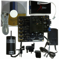
KIT DEV FOR Z8 ENCORE Z8FMC16100
Manufacturer
Zilog
Series
Z8 Encore! MC™r
Datasheets
1.Z8FMC160100KIT.pdf
(7 pages)
2.Z8FMC160100KIT.pdf
(383 pages)
3.Z8FMC160100KITG.pdf
(2 pages)
4.Z8FMC160100KITG.pdf
(15 pages)
Specifications of Z8FMC160100KITG
Main Purpose
Power Management, Motor Control
Embedded
Yes, MCU, 8-Bit
Utilized Ic / Part
Z8FMC16100
Primary Attributes
3-Ph DC Motors
Secondary Attributes
Graphical User Interface
For Use With
269-4664 - KIT ACC OPTO-ISO USB SMART CABLE269-4661 - KIT ACC ETHERNET SMART CABLE269-4539 - KIT ACCESSORY USB SMART CABLE
Lead Free Status / RoHS Status
Lead free / RoHS Compliant
Other names
269-4660


Z8FMC16100 Series Flash MCU
Product Specification
150
serial clock. The master drives the serial clock through its own serial clock (SCK) pin to the
slave’s SCK pin. When the SPI is configured as a slave, the SCK pin is an input and the
clock signal from the master synchronizes the data transfer between the master and slave
devices. These slave devices ignore the SCK signal unless the SS pin is asserted. When con-
figured as a slave, the SPI block requires a minimum SCK period of greater than or equal to
8 times the system (X
) clock period.
IN
The master and slave are each capable of exchanging a character of data during a sequence
of NUMBITS clock cycles (refer to the NUMBITS field in the SPIMODE register). In both
master and slave SPI devices, data is shifted on one edge of the SCK and is sampled on the
opposite edge, where data is stable. Edge polarity is determined by the SPI phase and
polarity control.
Slave Select
The active Low Slave Select (SS) input signal selects a slave SPI device. SS must be Low
prior to all data communication to and from the slave device. SS must remain Low for the
full duration of each character transferred. The SS signal may stay Low during the transfer
of multiple characters, or may deassert between each character.
When the SPI is configured as the only master in an SPI system, the SS pin can be set as
®
either an input or an output. For communication between the Z8 Encore!
8K Series
device’s SPI master and external slave devices, the SS signal, as an output, can assert the
SS input pin on one of the slave devices. Other GPIO output pins can also be employed to
select external SPI slave devices.
When the SPI is configured as one master in a multimaster SPI system, the SS pin should
be set as an input. The SS input signal on the master must be High. If the SS signal goes
Low (indicating that another master is driving the SPI bus), a collision error flag is set in
the SPI Status register.
SPI Clock Phase and Polarity Control
The SPI supports four combinations of serial clock phase and polarity using two bits in the
SPI Control register. The clock polarity bit, CLKPOL, selects an active High or active Low
clock and has no effect on the transfer format.
Table 83
lists the SPI Clock Phase and Polar-
ity Operation parameters. The clock phase bit, PHASE, selects one of two fundamentally
different transfer formats. For proper data transmission, clock phase and polarity must be
identical for the SPI master and the SPI slave. The master always places data on the MOSI
line a half-cycle before the receive clock edge (SCK signal) for the slave to latch the data.
PS024613-0910
SPI Clock Phase and Polarity Control
Related parts for Z8FMC160100KITG
Image
Part Number
Description
Manufacturer
Datasheet
Request
R

Part Number:
Description:
Communication Controllers, ZILOG INTELLIGENT PERIPHERAL CONTROLLER (ZIP)
Manufacturer:
Zilog, Inc.
Datasheet:

Part Number:
Description:
KIT DEV FOR Z8 ENCORE 16K TO 64K
Manufacturer:
Zilog
Datasheet:

Part Number:
Description:
KIT DEV Z8 ENCORE XP 28-PIN
Manufacturer:
Zilog
Datasheet:

Part Number:
Description:
DEV KIT FOR Z8 ENCORE 8K/4K
Manufacturer:
Zilog
Datasheet:

Part Number:
Description:
KIT DEV Z8 ENCORE XP 28-PIN
Manufacturer:
Zilog
Datasheet:

Part Number:
Description:
DEV KIT FOR Z8 ENCORE 4K TO 8K
Manufacturer:
Zilog
Datasheet:
Part Number:
Description:
CMOS Z8 microcontroller. ROM 16 Kbytes, RAM 256 bytes, speed 16 MHz, 32 lines I/O, 3.0V to 5.5V
Manufacturer:
Zilog, Inc.
Datasheet:
Part Number:
Description:
Low-cost microcontroller. 512 bytes ROM, 61 bytes RAM, 8 MHz
Manufacturer:
Zilog, Inc.
Datasheet:
Part Number:
Description:
Z8 4K OTP Microcontroller
Manufacturer:
Zilog, Inc.
Datasheet:
Part Number:
Description:
CMOS SUPER8 ROMLESS MCU
Manufacturer:
Zilog, Inc.
Datasheet:
Part Number:
Description:
SL1866 CMOSZ8 OTP Microcontroller
Manufacturer:
Zilog, Inc.
Datasheet:
Part Number:
Description:
SL1866 CMOSZ8 OTP Microcontroller
Manufacturer:
Zilog, Inc.
Datasheet:
Part Number:
Description:
OTP (KB) = 1, RAM = 125, Speed = 12, I/O = 14, 8-bit Timers = 2, Comm Interfaces Other Features = Por, LV Protect, Voltage = 4.5-5.5V
Manufacturer:
Zilog, Inc.
Datasheet:
Part Number:
Description:
Manufacturer:
Zilog, Inc.
Datasheet: