Z8FMC160100KITG Zilog, Z8FMC160100KITG Datasheet - Page 83
Z8FMC160100KITG
Manufacturer Part Number
Z8FMC160100KITG
Description
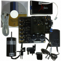
KIT DEV FOR Z8 ENCORE Z8FMC16100
Manufacturer
Zilog
Series
Z8 Encore! MC™r
Datasheets
1.Z8FMC160100KIT.pdf
(7 pages)
2.Z8FMC160100KIT.pdf
(383 pages)
3.Z8FMC160100KITG.pdf
(2 pages)
4.Z8FMC160100KITG.pdf
(15 pages)
Specifications of Z8FMC160100KITG
Main Purpose
Power Management, Motor Control
Embedded
Yes, MCU, 8-Bit
Utilized Ic / Part
Z8FMC16100
Primary Attributes
3-Ph DC Motors
Secondary Attributes
Graphical User Interface
For Use With
269-4664 - KIT ACC OPTO-ISO USB SMART CABLE269-4661 - KIT ACC ETHERNET SMART CABLE269-4539 - KIT ACCESSORY USB SMART CABLE
Lead Free Status / RoHS Status
Lead free / RoHS Compliant
Other names
269-4660


PS024613-0910
Minimum PWM Pulse Width Filter
Synchronization of PWM and Analog-to-Digital Converter
width of this deadband is attributed to the number of system clock cycles specified in the
PWM Deadband register (PWMDB). The minimum deadband duration is one system
clock, and the maximum duration is 255 system clocks. During the deadband period, both
PWM outputs of a complementary pair are deasserted. The generation of deadband time
does not alter the PWM period; instead, the deadband time is subtracted from the active
time of the PWM outputs.
the PWM output.
The PWM modulator is capable of producing pulses as narrow as a single system clock
cycle in width. As the response time of external drive circuits can be slower than the
period of a system clock, a filter is implemented to enforce a minimum-width pulse on the
PWM output pins. All output pulses, whether High or Low, must be at least the minimum
number of PWM clock cycles (for more details, see
as specified in the PWM Minimum Pulse Width Filter (PWMMPF) register. If the
expected pulse width is less than the threshold, the associated PWM output does not
change state until the duty cycle value has changed sufficiently to allow pulse generation
of an acceptable width. The minimum pulse width filter also accounts for the duty cycle
variation caused by the deadband insertion. The PWM output pulse is filtered even if the
programmed duty cycle is greater than the threshold, but the pulse width decrease because
of deadband insertion causes the pulse to be too narrow. The pulse width filter value is
calculated as:
where
The PWM Minimum Pulse Width Filter register can only be written when the
cleared. Values written to this register when
The ADC on the Z8FMC16100 Series Flash MCU can be synchronized with the PWM
period. Enabling the PWM ADC trigger causes the PWM to generate an ADC conversion
signal at the end of each PWM period. Additionally, in center-aligned mode, the PWM
generates a trigger at the center of the period. Setting the ADCTRIG bit in the PWM
Control 0 register (PWMCTL0) enables ADC synchronization.
Roundup (PWMMPF)
T
MINPULSEOUT
is the shortest allowed pulse width on the PWM outputs, in seconds.
=
Figure 8
T
SYSTEMCLOCK
and
Figure 9
T
MINPULSEOUT
PWEN
x PWM
display the effect of deadband insertion on
is set will be ignored.
PWM Prescaler on page
Z8FMC16100 Series Flash MCU
PRESCALER
Minimum PWM Pulse Width Filter
Product Specification
68) in width
PWEN
bit is
71
Related parts for Z8FMC160100KITG
Image
Part Number
Description
Manufacturer
Datasheet
Request
R

Part Number:
Description:
Communication Controllers, ZILOG INTELLIGENT PERIPHERAL CONTROLLER (ZIP)
Manufacturer:
Zilog, Inc.
Datasheet:

Part Number:
Description:
KIT DEV FOR Z8 ENCORE 16K TO 64K
Manufacturer:
Zilog
Datasheet:

Part Number:
Description:
KIT DEV Z8 ENCORE XP 28-PIN
Manufacturer:
Zilog
Datasheet:

Part Number:
Description:
DEV KIT FOR Z8 ENCORE 8K/4K
Manufacturer:
Zilog
Datasheet:

Part Number:
Description:
KIT DEV Z8 ENCORE XP 28-PIN
Manufacturer:
Zilog
Datasheet:

Part Number:
Description:
DEV KIT FOR Z8 ENCORE 4K TO 8K
Manufacturer:
Zilog
Datasheet:
Part Number:
Description:
CMOS Z8 microcontroller. ROM 16 Kbytes, RAM 256 bytes, speed 16 MHz, 32 lines I/O, 3.0V to 5.5V
Manufacturer:
Zilog, Inc.
Datasheet:
Part Number:
Description:
Low-cost microcontroller. 512 bytes ROM, 61 bytes RAM, 8 MHz
Manufacturer:
Zilog, Inc.
Datasheet:
Part Number:
Description:
Z8 4K OTP Microcontroller
Manufacturer:
Zilog, Inc.
Datasheet:
Part Number:
Description:
CMOS SUPER8 ROMLESS MCU
Manufacturer:
Zilog, Inc.
Datasheet:
Part Number:
Description:
SL1866 CMOSZ8 OTP Microcontroller
Manufacturer:
Zilog, Inc.
Datasheet:
Part Number:
Description:
SL1866 CMOSZ8 OTP Microcontroller
Manufacturer:
Zilog, Inc.
Datasheet:
Part Number:
Description:
OTP (KB) = 1, RAM = 125, Speed = 12, I/O = 14, 8-bit Timers = 2, Comm Interfaces Other Features = Por, LV Protect, Voltage = 4.5-5.5V
Manufacturer:
Zilog, Inc.
Datasheet:
Part Number:
Description:
Manufacturer:
Zilog, Inc.
Datasheet: