Z8FMC160100KITG Zilog, Z8FMC160100KITG Datasheet - Page 183
Z8FMC160100KITG
Manufacturer Part Number
Z8FMC160100KITG
Description
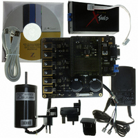
KIT DEV FOR Z8 ENCORE Z8FMC16100
Manufacturer
Zilog
Series
Z8 Encore! MC™r
Datasheets
1.Z8FMC160100KIT.pdf
(7 pages)
2.Z8FMC160100KIT.pdf
(383 pages)
3.Z8FMC160100KITG.pdf
(2 pages)
4.Z8FMC160100KITG.pdf
(15 pages)
Specifications of Z8FMC160100KITG
Main Purpose
Power Management, Motor Control
Embedded
Yes, MCU, 8-Bit
Utilized Ic / Part
Z8FMC16100
Primary Attributes
3-Ph DC Motors
Secondary Attributes
Graphical User Interface
For Use With
269-4664 - KIT ACC OPTO-ISO USB SMART CABLE269-4661 - KIT ACC ETHERNET SMART CABLE269-4539 - KIT ACCESSORY USB SMART CABLE
Lead Free Status / RoHS Status
Lead free / RoHS Compliant
Other names
269-4660


PS024613-0910
Read/Write control bit (which is cleared to 0). The transmit operation is performed in the
same manner as 7-bit addressing.
The procedure for a master transmit operation to a 10-bit addressed slave is as follows:
1. The software initializes the
2. The software asserts the
3. The I
4. The software responds to the TDRE interrupt by writing the first slave address byte
5. The software asserts the
6. The I
7. The I
8. After one bit of the address is shifted out by the SDA signal, the transmit interrupt
9. The software responds by writing the second byte of address into the contents of the
10. The I
11. The I
12. The I
13. The I
14. The software responds by writing the data to be written out to the I
mode with 7- or 10-bit addressing (the I
address types). The
as a slave (but not for the remote slave). The software asserts the IEN bit in the I
Control register.
interrupts.
(
register.
asserts.
I
out via the SDA signal.
High period of SCL. The I
If the slave does not acknowledge the first address byte, the I
NCKI bit in the I
State register. The software responds to the Not Acknowledge interrupt by setting the
STOP
from the data register, sends a
NCKI
register (2nd address byte).
first bit has been sent, the transmit interrupt asserts.
11110xx0
2
C Data register.
2
2
2
2
2
2
2
bit and clearing the
bits. The transaction is complete, and the following steps can be ignored.
C controller shifts the remainder of the first byte of the address and the Write bit
C interrupt asserts because the I
C controller sends a
C controller loads the I
C slave sends an Acknowledge by pulling the SDA signal Low during the next
C controller loads the I
C controller shifts the second address byte out via the SDA signal. After the
). The least-significant bit must be 0 for the write operation.
2
C Status register, sets the
MODE
TXI
START
field selects the address width for this mode when addressed
TXI
2
START
MODE
C controller sets the ACK bit in the I
bit of the I
2
2
C Shift register with the contents of the I
C Shift register with the contents of the I
STOP
bit. The I
bit of the I
field in the I
condition to the I
condition on the bus, and clears the
2
C Data register is empty.
2
2
2
C bus protocol allows the mixing of slave
C Control register to enable transmit
C controller flushes the second address byte
2
ACKV
C Control register.
2
C Mode register for MASTER/SLAVE
Z8FMC16100 Series Flash MCU
bit, and clears the
2
C slave.
Product Specification
2
C controller sets the
2
C Status register.
2
Master Transactions
C Control register.
ACK
2
2
C Data
C Data
bit in the I
STOP
and
2
C
2
C
171
Related parts for Z8FMC160100KITG
Image
Part Number
Description
Manufacturer
Datasheet
Request
R

Part Number:
Description:
Communication Controllers, ZILOG INTELLIGENT PERIPHERAL CONTROLLER (ZIP)
Manufacturer:
Zilog, Inc.
Datasheet:

Part Number:
Description:
KIT DEV FOR Z8 ENCORE 16K TO 64K
Manufacturer:
Zilog
Datasheet:

Part Number:
Description:
KIT DEV Z8 ENCORE XP 28-PIN
Manufacturer:
Zilog
Datasheet:

Part Number:
Description:
DEV KIT FOR Z8 ENCORE 8K/4K
Manufacturer:
Zilog
Datasheet:

Part Number:
Description:
KIT DEV Z8 ENCORE XP 28-PIN
Manufacturer:
Zilog
Datasheet:

Part Number:
Description:
DEV KIT FOR Z8 ENCORE 4K TO 8K
Manufacturer:
Zilog
Datasheet:
Part Number:
Description:
CMOS Z8 microcontroller. ROM 16 Kbytes, RAM 256 bytes, speed 16 MHz, 32 lines I/O, 3.0V to 5.5V
Manufacturer:
Zilog, Inc.
Datasheet:
Part Number:
Description:
Low-cost microcontroller. 512 bytes ROM, 61 bytes RAM, 8 MHz
Manufacturer:
Zilog, Inc.
Datasheet:
Part Number:
Description:
Z8 4K OTP Microcontroller
Manufacturer:
Zilog, Inc.
Datasheet:
Part Number:
Description:
CMOS SUPER8 ROMLESS MCU
Manufacturer:
Zilog, Inc.
Datasheet:
Part Number:
Description:
SL1866 CMOSZ8 OTP Microcontroller
Manufacturer:
Zilog, Inc.
Datasheet:
Part Number:
Description:
SL1866 CMOSZ8 OTP Microcontroller
Manufacturer:
Zilog, Inc.
Datasheet:
Part Number:
Description:
OTP (KB) = 1, RAM = 125, Speed = 12, I/O = 14, 8-bit Timers = 2, Comm Interfaces Other Features = Por, LV Protect, Voltage = 4.5-5.5V
Manufacturer:
Zilog, Inc.
Datasheet:
Part Number:
Description:
Manufacturer:
Zilog, Inc.
Datasheet: