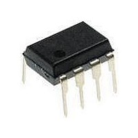
PIC12F1840-I/P Microchip Technology, PIC12F1840-I/P Datasheet - Page 105

PIC12F1840-I/P
Manufacturer Part Number
PIC12F1840-I/P
Description
7 KB Flash, 256 Bytes RAM, 32 MHz Int. Osc, 6 I/0, Enhanced Mid Range Core 8 PDI
Manufacturer
Microchip Technology
Datasheet
1.PIC12F1840-IP.pdf
(382 pages)
Specifications of PIC12F1840-I/P
Processor Series
PIC12F
Core
PIC
Program Memory Type
Flash
Program Memory Size
7 KB
Data Ram Size
256 B
Interface Type
MI2C, SPI, EUSART
Number Of Timers
3
Operating Supply Voltage
1.8 V to 5.5 V
Maximum Operating Temperature
+ 85 C
Mounting Style
Through Hole
Package / Case
PDIP-8
Development Tools By Supplier
MPLAB IDE Software
Minimum Operating Temperature
- 40 C
Lead Free Status / Rohs Status
Lead free / RoHS Compliant
Available stocks
Company
Part Number
Manufacturer
Quantity
Price
Company:
Part Number:
PIC12F1840-I/P
Manufacturer:
MICROCHIP
Quantity:
200
- Current page: 105 of 382
- Download datasheet (4Mb)
EXAMPLE 11-5:
2011 Microchip Technology Inc.
; This write routine assumes the following:
; 1. The 64 bytes of data are loaded, starting at the address in DATA_ADDR
; 2. Each word of data to be written is made up of two adjacent bytes in DATA_ADDR,
;
; 3. A valid starting address (the least significant bits = 00000) is loaded in ADDRH:ADDRL
; 4. ADDRH and ADDRL are located in shared data memory 0x70 - 0x7F
;
LOOP
START_WRITE
stored in little endian format
BCF
BANKSEL
MOVF
MOVWF
MOVF
MOVWF
MOVLW
MOVWF
MOVLW
MOVWF
BSF
BCF
BSF
BSF
MOVIW
MOVWF
MOVIW
MOVWF
MOVF
XORLW
ANDLW
BTFSC
GOTO
MOVLW
MOVWF
MOVLW
MOVWF
BSF
NOP
NOP
INCF
GOTO
BCF
MOVLW
MOVWF
MOVLW
MOVWF
BSF
NOP
NOP
BCF
BSF
WRITING TO FLASH PROGRAM MEMORY
INTCON,GIE
EEADRH
ADDRH,W
EEADRH
ADDRL,W
EEADRL
LOW DATA_ADDR
FSR0L
HIGH DATA_ADDR ; Load initial data address
FSR0H
EECON1,EEPGD
EECON1,CFGS
EECON1,WREN
EECON1,LWLO
FSR0++
EEDATL
FSR0++
EEDATH
EEADRL,W
0x1F
0x1F
STATUS,Z
START_WRITE
55h
EECON2
0AAh
EECON2
EECON1,WR
EEADRL,F
LOOP
EECON1,LWLO
55h
EECON2
0AAh
EECON2
EECON1,WR
EECON1,WREN
INTCON,GIE
; Disable ints so required sequences will execute properly
; Bank 3
; Load initial address
;
;
;
; Load initial data address
;
;
; Point to program memory
; Not configuration space
; Enable writes
; Only Load Write Latches
; Load first data byte into lower
;
; Load second data byte into upper
;
; Check if lower bits of address are '00000'
; Check if we're on the last of 32 addresses
;
; Exit if last of 32 words,
;
; Start of required write sequence:
; Write 55h
;
; Write AAh
; Set WR bit to begin write
; Any instructions here are ignored as processor
; halts to begin write sequence
; Processor will stop here and wait for write to complete.
; After write processor continues with 3rd instruction.
; Still loading latches Increment address
; Write next latches
; No more loading latches - Actually start Flash program
; memory write
; Start of required write sequence:
; Write 55h
;
; Write AAh
; Set WR bit to begin write
; Any instructions here are ignored as processor
; halts to begin write sequence
; Processor will stop here and wait for write complete.
; after write processor continues with 3rd instruction
; Disable writes
; Enable interrupts
Preliminary
PIC12(L)F1840
DS41441B-page 105
Related parts for PIC12F1840-I/P
Image
Part Number
Description
Manufacturer
Datasheet
Request
R

Part Number:
Description:
7 KB Flash, 256 Bytes RAM, 32 MHz Int. Osc, 6 I/0, Enhanced Mid Range Core, Nano
Manufacturer:
Microchip Technology
Datasheet:

Part Number:
Description:
MCU, MPU & DSP Development Tools 8 Bit PIC Develop Microcontroller
Manufacturer:
SchmartBoard
Datasheet:

Part Number:
Description:
7 KB Flash, 256 Bytes RAM, 32 MHz Int. Osc, 6 I/0, Enhanced Mid Range Core 8 DFN
Manufacturer:
Microchip Technology

Part Number:
Description:
7 KB Flash, 256 Bytes RAM, 32 MHz Int. Osc, 6 I/0, Enhanced Mid Range Core 8 SOI
Manufacturer:
Microchip Technology

Part Number:
Description:
7 KB Flash, 256 Bytes RAM, 32 MHz Int. Osc, 6 I/0, Enhanced Mid Range Core, Nano
Manufacturer:
Microchip Technology
Datasheet:

Part Number:
Description:
7 KB Flash, 256 Bytes RAM, 32 MHz Int. Osc, 6 I/0, Enhanced Mid Range Core, Nano
Manufacturer:
Microchip Technology
Datasheet:

Part Number:
Description:
7 KB Flash, 256 Bytes RAM, 32 MHz Int. Osc, 6 I/0, Enhanced Mid Range Core, Nano
Manufacturer:
Microchip Technology
Datasheet:

Part Number:
Description:
7 KB Flash, 256 Bytes RAM, 32 MHz Int. Osc, 6 I/0, Enhanced Mid Range Core, Nano
Manufacturer:
Microchip Technology

Part Number:
Description:
7 KB Flash, 256 Bytes RAM, 32 MHz Int. Osc, 6 I/0, Enhanced Mid Range Core, Nano
Manufacturer:
Microchip Technology

Part Number:
Description:
7 KB Flash, 256 Bytes RAM, 32 MHz Int. Osc, 6 I/0, Enhanced Mid Range Core, Nano
Manufacturer:
Microchip Technology
Datasheet:

Part Number:
Description:
7 KB Flash, 256 Bytes RAM, 32 MHz Int. Osc, 6 I/0, Enhanced Mid Range Core, Nano
Manufacturer:
Microchip Technology
Datasheet:

Part Number:
Description:
Manufacturer:
Microchip Technology Inc.
Datasheet:

Part Number:
Description:
Manufacturer:
Microchip Technology Inc.
Datasheet:


