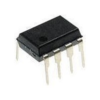
PIC12F1840-I/P Microchip Technology, PIC12F1840-I/P Datasheet - Page 191

PIC12F1840-I/P
Manufacturer Part Number
PIC12F1840-I/P
Description
7 KB Flash, 256 Bytes RAM, 32 MHz Int. Osc, 6 I/0, Enhanced Mid Range Core 8 PDI
Manufacturer
Microchip Technology
Datasheet
1.PIC12F1840-IP.pdf
(382 pages)
Specifications of PIC12F1840-I/P
Processor Series
PIC12F
Core
PIC
Program Memory Type
Flash
Program Memory Size
7 KB
Data Ram Size
256 B
Interface Type
MI2C, SPI, EUSART
Number Of Timers
3
Operating Supply Voltage
1.8 V to 5.5 V
Maximum Operating Temperature
+ 85 C
Mounting Style
Through Hole
Package / Case
PDIP-8
Development Tools By Supplier
MPLAB IDE Software
Minimum Operating Temperature
- 40 C
Lead Free Status / Rohs Status
Lead free / RoHS Compliant
Available stocks
Company
Part Number
Manufacturer
Quantity
Price
Company:
Part Number:
PIC12F1840-I/P
Manufacturer:
MICROCHIP
Quantity:
200
- Current page: 191 of 382
- Download datasheet (4Mb)
24.1.5
Capture mode depends upon the Timer1 module for
proper operation. There are two options for driving the
Timer1 module in Capture mode. It can be driven by the
instruction clock (F
When Timer1 is clocked by F
increment during Sleep. When the device wakes from
Sleep, Timer1 will continue from its previous state.
Capture mode will operate during Sleep when Timer1
is clocked by an external clock source.
TABLE 24-2:
2011 Microchip Technology Inc.
APFCON
CCP1CON
CCPR1L
CCPR1H
INTCON
PIE1
PIE2
PIR1
PIR2
T1CON
T1GCON
TMR1L
TMR1H
TRISA
Legend: — = Unimplemented location, read as ‘0’. Shaded cells are not used by Capture mode.
Name
*
Page provides register information.
CAPTURE DURING SLEEP
Capture/Compare/PWM Register 1 Low Byte (LSB)
Capture/Compare/PWM Register 1 High Byte (MSB)
Holding Register for the Least Significant Byte of the 16-bit TMR1 Register
Holding Register for the Most Significant Byte of the 16-bit TMR1 Register
RXDTSEL
TMR1GIE
TMR1GIF
TMR1GE
OSFIE
OSFIF
Bit 7
GIE
TMR1CS<1:0>
—
OSC
SUMMARY OF REGISTERS ASSOCIATED WITH CAPTURE
P1M<1:0>
/4), or by an external clock source.
SDOSEL
T1GPOL
PEIE
ADIE
ADIF
Bit 6
—
—
—
OSC
/4, Timer1 will not
TMR0IE
T1GTM
TRISA5
SSSEL
RCIE
RCIF
C1IE
Bit 5
C1IF
T1CKPS<1:0>
DC1B<1:0>
T1GSPM
TRISA4
INTE
EEIE
Bit 4
TXIE
TXIF
EEIF
—
Preliminary
T1GGO/DONE
T1OSCEN
T1GSEL
SSP1IE
TRISA3
BCL1IE
SSP1IF
BCL1IF
IOCIE
Bit 3
24.1.6
This module incorporates I/O pins that can be moved to
other locations with the use of the alternate pin function
register, APFCON. To determine which pins can be
moved and what their default locations are upon a
reset, see
more information.
TXCKSEL
T1SYNC
Section 12.1 “Alternate Pin Function”
T1GVAL
TMR0IF
CCP1IE
CCP1IF
TRISA2
ALTERNATE PIN LOCATIONS
Bit 2
CCP1M<3:0>
—
—
PIC12(L)F1840
P1BSEL
TMR2IE
TMR2IF
TRISA1
INTF
Bit 1
—
—
—
T1GSS<1:0>
CCP1SEL
TMR1ON
TMR1IE
TMR1IF
TRISA0
IOCIF
Bit 0
DS41441B-page 191
—
—
Register
on Page
167*
167*
112
207
190
190
171
172
115
83
84
85
86
87
for
Related parts for PIC12F1840-I/P
Image
Part Number
Description
Manufacturer
Datasheet
Request
R

Part Number:
Description:
7 KB Flash, 256 Bytes RAM, 32 MHz Int. Osc, 6 I/0, Enhanced Mid Range Core, Nano
Manufacturer:
Microchip Technology
Datasheet:

Part Number:
Description:
MCU, MPU & DSP Development Tools 8 Bit PIC Develop Microcontroller
Manufacturer:
SchmartBoard
Datasheet:

Part Number:
Description:
7 KB Flash, 256 Bytes RAM, 32 MHz Int. Osc, 6 I/0, Enhanced Mid Range Core 8 DFN
Manufacturer:
Microchip Technology

Part Number:
Description:
7 KB Flash, 256 Bytes RAM, 32 MHz Int. Osc, 6 I/0, Enhanced Mid Range Core 8 SOI
Manufacturer:
Microchip Technology

Part Number:
Description:
7 KB Flash, 256 Bytes RAM, 32 MHz Int. Osc, 6 I/0, Enhanced Mid Range Core, Nano
Manufacturer:
Microchip Technology
Datasheet:

Part Number:
Description:
7 KB Flash, 256 Bytes RAM, 32 MHz Int. Osc, 6 I/0, Enhanced Mid Range Core, Nano
Manufacturer:
Microchip Technology
Datasheet:

Part Number:
Description:
7 KB Flash, 256 Bytes RAM, 32 MHz Int. Osc, 6 I/0, Enhanced Mid Range Core, Nano
Manufacturer:
Microchip Technology
Datasheet:

Part Number:
Description:
7 KB Flash, 256 Bytes RAM, 32 MHz Int. Osc, 6 I/0, Enhanced Mid Range Core, Nano
Manufacturer:
Microchip Technology

Part Number:
Description:
7 KB Flash, 256 Bytes RAM, 32 MHz Int. Osc, 6 I/0, Enhanced Mid Range Core, Nano
Manufacturer:
Microchip Technology

Part Number:
Description:
7 KB Flash, 256 Bytes RAM, 32 MHz Int. Osc, 6 I/0, Enhanced Mid Range Core, Nano
Manufacturer:
Microchip Technology
Datasheet:

Part Number:
Description:
7 KB Flash, 256 Bytes RAM, 32 MHz Int. Osc, 6 I/0, Enhanced Mid Range Core, Nano
Manufacturer:
Microchip Technology
Datasheet:

Part Number:
Description:
Manufacturer:
Microchip Technology Inc.
Datasheet:

Part Number:
Description:
Manufacturer:
Microchip Technology Inc.
Datasheet:


