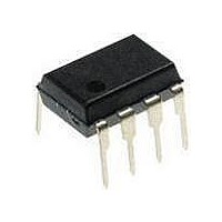
PIC12F1840-I/P Microchip Technology, PIC12F1840-I/P Datasheet - Page 111

PIC12F1840-I/P
Manufacturer Part Number
PIC12F1840-I/P
Description
7 KB Flash, 256 Bytes RAM, 32 MHz Int. Osc, 6 I/0, Enhanced Mid Range Core 8 PDI
Manufacturer
Microchip Technology
Datasheet
1.PIC12F1840-IP.pdf
(382 pages)
Specifications of PIC12F1840-I/P
Processor Series
PIC12F
Core
PIC
Program Memory Type
Flash
Program Memory Size
7 KB
Data Ram Size
256 B
Interface Type
MI2C, SPI, EUSART
Number Of Timers
3
Operating Supply Voltage
1.8 V to 5.5 V
Maximum Operating Temperature
+ 85 C
Mounting Style
Through Hole
Package / Case
PDIP-8
Development Tools By Supplier
MPLAB IDE Software
Minimum Operating Temperature
- 40 C
Lead Free Status / Rohs Status
Lead free / RoHS Compliant
Available stocks
Company
Part Number
Manufacturer
Quantity
Price
Company:
Part Number:
PIC12F1840-I/P
Manufacturer:
MICROCHIP
Quantity:
200
- Current page: 111 of 382
- Download datasheet (4Mb)
12.0
In general, when a peripheral is enabled, that pin may
not be used as a general purpose I/O pin.
The port has three registers for its operation. These
registers are:
• TRISA register (data direction register)
• PORTA register (reads the levels on the pins of
• LATA register (output latch)
PORTA has the following additional registers. They
are:
• ANSELA (analog select)
• WPUA (weak pull-up)
The Data Latch (LATA register) is useful for
read-modify-write operations on the value that the I/O
pins are driving.
A write operation to the LATA register has the same
affect as a write to the corresponding PORTA register.
A read of the LATA register reads of the values held in
the I/O PORT latches, while a read of the PORTA
register reads the actual I/O pin value.
The port has analog functions and has an ANSELA.
register which can disable the digital input and save
power. A simplified model of a generic I/O port, without
the interfaces to other peripherals, is shown in
Figure
FIGURE 12-1:
2011 Microchip Technology Inc.
To peripherals
Write LATA
Write PORTA
Data Bus
the device)
Read PORTA
12-1.
I/O PORTS
Data Register
D
CK
Read LATA
ANSELA
GENERIC I/O PORT
OPERATION
Q
TRISA
V
V
DD
SS
I/O pin
Preliminary
12.1
The Alternate Pin Function Control (APFCON) register
is used to steer specific peripheral input and output
functions between different pins. The APFCON register
is shown in
following functions can be moved between different
pins.
• RX/DT
• TX/CK
• SDO
• SS (Slave Select)
• T1G
• P1B
• CCP1/P1A
These bits have no effect on the values of any TRIS
register. PORT and TRIS overrides will be routed to the
correct pin. The unselected pin will be unaffected.
Alternate Pin Function
Register
PIC12(L)F1840
12-1. For this device family, the
DS41441B-page 111
Related parts for PIC12F1840-I/P
Image
Part Number
Description
Manufacturer
Datasheet
Request
R

Part Number:
Description:
7 KB Flash, 256 Bytes RAM, 32 MHz Int. Osc, 6 I/0, Enhanced Mid Range Core, Nano
Manufacturer:
Microchip Technology
Datasheet:

Part Number:
Description:
MCU, MPU & DSP Development Tools 8 Bit PIC Develop Microcontroller
Manufacturer:
SchmartBoard
Datasheet:

Part Number:
Description:
7 KB Flash, 256 Bytes RAM, 32 MHz Int. Osc, 6 I/0, Enhanced Mid Range Core 8 DFN
Manufacturer:
Microchip Technology

Part Number:
Description:
7 KB Flash, 256 Bytes RAM, 32 MHz Int. Osc, 6 I/0, Enhanced Mid Range Core 8 SOI
Manufacturer:
Microchip Technology

Part Number:
Description:
7 KB Flash, 256 Bytes RAM, 32 MHz Int. Osc, 6 I/0, Enhanced Mid Range Core, Nano
Manufacturer:
Microchip Technology
Datasheet:

Part Number:
Description:
7 KB Flash, 256 Bytes RAM, 32 MHz Int. Osc, 6 I/0, Enhanced Mid Range Core, Nano
Manufacturer:
Microchip Technology
Datasheet:

Part Number:
Description:
7 KB Flash, 256 Bytes RAM, 32 MHz Int. Osc, 6 I/0, Enhanced Mid Range Core, Nano
Manufacturer:
Microchip Technology
Datasheet:

Part Number:
Description:
7 KB Flash, 256 Bytes RAM, 32 MHz Int. Osc, 6 I/0, Enhanced Mid Range Core, Nano
Manufacturer:
Microchip Technology

Part Number:
Description:
7 KB Flash, 256 Bytes RAM, 32 MHz Int. Osc, 6 I/0, Enhanced Mid Range Core, Nano
Manufacturer:
Microchip Technology

Part Number:
Description:
7 KB Flash, 256 Bytes RAM, 32 MHz Int. Osc, 6 I/0, Enhanced Mid Range Core, Nano
Manufacturer:
Microchip Technology
Datasheet:

Part Number:
Description:
7 KB Flash, 256 Bytes RAM, 32 MHz Int. Osc, 6 I/0, Enhanced Mid Range Core, Nano
Manufacturer:
Microchip Technology
Datasheet:

Part Number:
Description:
Manufacturer:
Microchip Technology Inc.
Datasheet:

Part Number:
Description:
Manufacturer:
Microchip Technology Inc.
Datasheet:


